Wafer Handling Robots Market Statistics & Forecasts 2026
Introduction
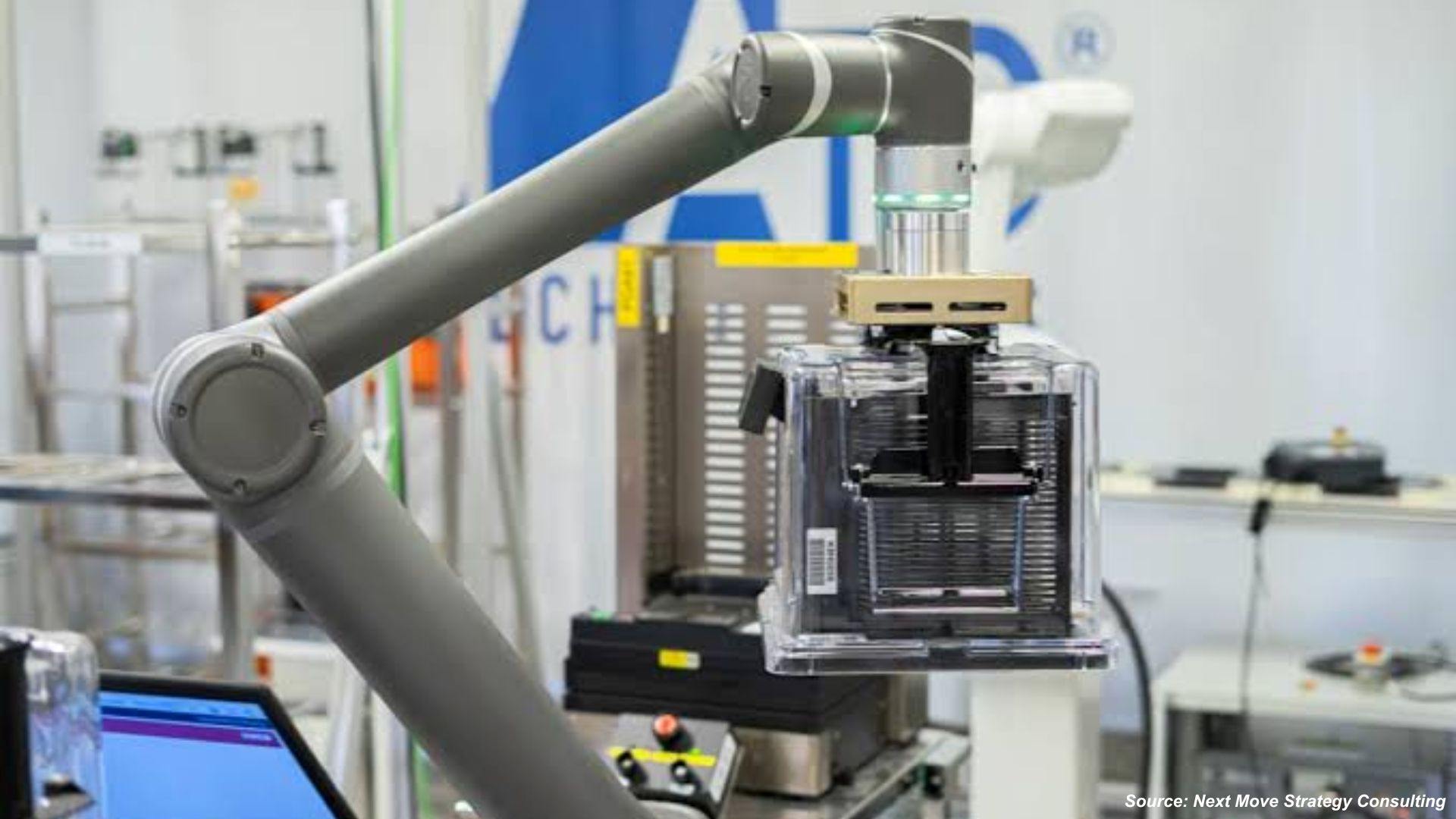
The global wafer handling robots market is navigating one of the most consequential periods in the history of semiconductor manufacturing. As governments race to secure domestic chip production capacity, geopolitical tensions reshape global supply chains, and artificial intelligence accelerates demand for advanced semiconductors, the specialized robotic systems that move, position, and protect delicate silicon wafers have become indispensable to the entire technology ecosystem.
According to Next Move Strategy Consulting (NMSC), the global Wafer Handling Robots Market is projected to reach USD 3.37 billion, registering a CAGR of 11.2% by 2030. This robust growth trajectory is being driven by a convergence of landmark policy developments — including the European Commission's Chips Act 2.0 proposal in June 2026 and the U.S. Section 232 semiconductor tariffs enacted in January 2026 — alongside an unprecedented global wave of semiconductor fab construction that is generating sustained, structural demand for precision automation solutions.
This article examines the most consequential trends, regulatory developments, and strategic implications defining the wafer handling robots market in 2026, providing C-level executives, investors, and procurement decision-makers with the intelligence required to navigate this rapidly evolving landscape.
For More Information: Download FREE Sample on Wafer Handling Robots Market Report
EU Chips Act 2.0 and U.S. Section 232 Tariffs: Twin Policy Forces Reshaping the Wafer Handling Robots Market
The European Commission's Chips Act 2.0: A New Strategic Framework
On June 3, 2026, the European Commission adopted a formal proposal for the Chips Act 2.0 — a landmark update to its 2023 semiconductor strategy — introducing new measures to further strengthen the Union's semiconductor ecosystem, reduce strategic dependencies, and scale critical manufacturing capacity across Europe.
The Chips Act 2.0 represents a significant escalation of Europe's industrial policy ambitions in the semiconductor sector. Key structural elements of the proposal include:
-
Accelerated permitting: A permit-granting cap of 12 months from a complete application, with a one-stop shop established in each EU Member State to streamline approvals for semiconductor manufacturing projects.
-
Expanded support for strategic projects: The proposal broadens the EU's toolkit for supporting strategic semiconductor projects, including those involving advanced wafer fabrication, packaging, and testing infrastructure.
-
Strengthened technological sovereignty: The framework is designed to reduce Europe's dependence on non-EU semiconductor supply chains, with particular emphasis on scaling domestic production of advanced chips used in automotive, defense, and AI applications.
-
Enhanced monitoring and crisis response: New mechanisms for monitoring supply chain vulnerabilities and coordinating crisis responses across Member States.
The Chips Act 2.0 directly catalyzes demand for wafer handling robots by incentivizing the construction and expansion of semiconductor fabs across Europe. Every new fab requires a fleet of precision robotic systems for wafer transport, alignment, and contamination-free handling — making the policy a direct demand driver for the market.
U.S. Section 232 Semiconductor Tariffs: A 25% Duty Reshaping Supply Chains
On January 14, 2026, President Trump issued a proclamation under Section 232 of the Trade Expansion Act of 1962, imposing a 25% ad valorem tariff on certain advanced computing chips and specified semiconductor manufacturing equipment, effective January 15, 2026. The proclamation also directed the Secretary of Commerce to provide an update by July 1, 2026, on the market for semiconductors used in the United States, signaling the potential for further regulatory action.
The Section 232 tariffs carry significant implications for the wafer handling robots market:
-
Accelerated domestic fab investment: The tariffs create a strong economic incentive for U.S. semiconductor companies to accelerate domestic manufacturing investment, reducing reliance on imported chips and equipment. This directly increases demand for wafer handling robots in new U.S. fabs.
-
Supply chain reconfiguration: Manufacturers of wafer handling robots with global supply chains must reassess component sourcing strategies to mitigate tariff exposure on semiconductor manufacturing equipment.
-
CHIPS Act synergy: The Section 232 tariffs reinforce the demand-side pull created by the CHIPS and Science Act of 2022, which appropriated USD 52.7 billion to increase semiconductor manufacturing capacity in the United States.
NMSC Strategic Perspective: Policy Convergence as a Market Accelerant
From Next Move Strategy Consulting's analytical standpoint, the simultaneous enactment of the EU Chips Act 2.0 and U.S. Section 232 tariffs represents a policy convergence that is structurally accelerating the global wafer handling robots market. Both measures — though distinct in mechanism — share a common outcome: the acceleration of domestic semiconductor manufacturing investment in their respective regions, each of which requires advanced automation infrastructure.
NMSC's assessment is that manufacturers of wafer handling robots with diversified geographic exposure, cleanroom-compliant product portfolios, and demonstrated AI integration capabilities are best positioned to capture the demand surge generated by this dual policy environment. The market's projected CAGR of 11.2% through 2030 reflects, in part, the sustained investment cycle that these policy frameworks are expected to generate.
Section Summary: The wafer handling robots market is being reshaped by two landmark policy developments in 2026: the EU Chips Act 2.0 (June 3, 2026), which accelerates European semiconductor manufacturing investment, and the U.S. Section 232 semiconductor tariffs (effective January 15, 2026), which impose a 25% duty on certain chips and manufacturing equipment.
-
The EU Chips Act 2.0 introduces a 12-month permit-granting cap and a one-stop shop in each Member State, directly accelerating fab construction timelines across Europe.
-
The U.S. Section 232 tariffs impose a 25% ad valorem duty on certain advanced computing chips and semiconductor manufacturing equipment, incentivizing domestic production investment.
-
The CHIPS and Science Act's USD 52.7 billion appropriation reinforces the demand-side pull for wafer handling robots in the United States.
Industry Impact Analysis
Global Fab Expansion: The Structural Demand Engine
The most consequential near-term driver of wafer handling robot demand is the unprecedented global wave of semiconductor fab construction. According to SEMI's World Fab Forecast, total installed semiconductor manufacturing capacity is expected to grow 5% in both 2026 and 2027, driven by sustained investment across North America, Europe, and Asia-Pacific. SEMI also reported that 18 new semiconductor fabs were scheduled to start construction in 2025, comprising three 200mm and fifteen 300mm facilities, the majority of which are expected to begin operations within the forecast period.
Each new fab represents a significant procurement event for wafer handling robot suppliers. A single 300mm fab typically requires hundreds of robotic wafer transfer systems across front-end lithography, etch, deposition, metrology, and back-end packaging stages. The scale of current fab construction activity therefore translates directly into a multi-year demand pipeline for the wafer handling robots market.
Deloitte's 2026 Global Semiconductor Industry Outlook notes that investments made in 2025 will likely continue or accelerate in 2026, creating a funding and demand ecosystem where capital expenditure commitments are translating into active equipment procurement cycles.
AI and Vision System Integration: Elevating Robot Intelligence
The wafer handling robots market is undergoing a fundamental technological transformation. Robots are evolving beyond traditional mechanical transport systems into intelligent, data-driven platforms. Integration of AI and machine learning enables robots to continuously analyze sensor data, detect defects, and adjust movement parameters in real time. Advanced vision systems now allow precise wafer alignment and detection of micro-contaminants that were previously difficult to identify.
Predictive maintenance powered by AI is extending robot life cycles and optimizing maintenance schedules, directly reducing operational costs for fab operators. The industry is moving toward collaborative robotic ecosystems where wafer handlers communicate with process tools, metrology equipment, and Manufacturing Execution Systems (MES), creating a fully connected smart fab environment aligned with Industry 4.0 objectives. This technological evolution is elevating the value proposition of wafer handling robots from commodity automation to strategic fab infrastructure.
The 300mm and Next-Generation Wafer Size Opportunity
The shift to larger wafer formats — with 300mm now the dominant standard and pilot projects underway for 450mm — is unlocking a significant product innovation opportunity for wafer handling robot suppliers. These next-generation processes demand robots with enhanced precision, improved edge-grip designs, and the ability to handle increasingly complex wafer stacks while maintaining contamination-free conditions.
The transition to 3D packaging technologies — including heterogeneous integration and chiplet architectures — further elevates the technical requirements for wafer handling systems, creating demand for modular, flexible robot designs with scalable payload capacity and adaptive end-effectors.
North America: CHIPS Act and Section 232 as Dual Demand Catalysts
North America is expected to show steady growth in the global wafer handling robots market, driven by rising government investments in semiconductor research and development, exemplified by the CHIPS and Science Act of 2022. International collaborations, such as the U.S.-India Memorandum of Understanding on semiconductor cooperation, further foster mutual growth in the sector. The rising adoption of electric vehicles in response to environmental regulations and consumer preferences also fuels demand for advanced semiconductor production equipment, including wafer handling robots, throughout the North American region.
Competitive Landscape: Strategic Moves in 2025–2026
The wafer handling robots market features a competitive landscape of established global players pursuing product innovation and strategic partnerships. Key market participants identified by NMSC include Brooks Automation, Inc., Kawasaki Heavy Industries Ltd., Yaskawa Electric Corporation, RORZE Corporation, DAIHEN Corporation, Nidec Corporation, Hirata Corporation, Kensington Laboratories LLC, Epson Robots (Seiko Epson), Hine Automation, JEL Corporation, Robostar Co., Ltd., Shibaura Machine Co., Ltd., Staubli International AG, HYULIM Robot Co., Ltd., RAONTEC Inc., ISEL Germany AG, Sanwa Engineering Corporation, HIWIN Technologies Corp., and He Five LLC.
Notable recent strategic developments include:
-
Kawasaki Heavy Industries Ltd. (July 2025): Launched the MC006V robot in the MC Series, enhancing cleanroom-compatible automation. The company also partnered with Foxconn to co-develop a medical assistant robot, highlighting its broader robotics expansion strategy.
-
Brooks Automation, Inc. (May 2024): Joined the Responsible Business Alliance while continuing to advance its Marathon® and MagnaTran® LEAP wafer-transfer platforms, reinforcing its commitment to sustainable and responsible supply chain practices.
Section Summary: The wafer handling robots market's growth is underpinned by an unprecedented global fab construction wave, accelerating AI integration, the transition to larger wafer formats, and active competitive dynamics across North America, Europe, and Asia-Pacific.
-
SEMI's World Fab Forecast projects total installed semiconductor capacity to grow 5% in both 2026 and 2027, with 18 new fabs having started construction in 2025.
-
AI and machine learning integration is transforming wafer handling robots from mechanical transport systems into intelligent, predictive automation platforms.
-
The shift to 300mm and next-generation wafer formats is creating a significant product innovation and replacement demand cycle for robot suppliers.
-
Asia-Pacific maintains its dominant regional position, while North America and Europe are experiencing policy-driven demand acceleration.
Pros and Cons of Recent Market Developments
|
Development |
Pros |
Cons |
|
EU Chips Act 2.0 (June 2026) |
Accelerates European fab construction; creates sustained demand for wafer handling robots; reduces EU dependency on non-European semiconductor supply chains |
Regulatory complexity for manufacturers entering new EU markets; permitting timelines, even with the 12-month cap, may delay fab commissioning |
|
U.S. Section 232 Semiconductor Tariffs (January 2026) |
Incentivizes domestic U.S. fab investment; strengthens demand for locally sourced automation equipment; reinforces CHIPS Act investment cycle |
Increases cost of imported semiconductor manufacturing equipment; creates supply chain disruption for robot manufacturers with global component sourcing; risk of retaliatory trade measures |
|
Global Fab Expansion (SEMI: 18 new fabs in 2025) |
Creates a multi-year demand pipeline for wafer handling robots; drives volume procurement across all robot types and wafer sizes |
Intensifies competition among robot suppliers; risk of overcapacity in certain wafer size segments; supply chain bottlenecks for specialized components |
|
AI and Vision System Integration |
Enables premium pricing; improves fab yield and defect detection; supports predictive maintenance and reduced downtime |
Higher upfront system cost; requires specialized workforce for programming and calibration; increases cybersecurity exposure in connected fab environments |
|
Transition to 300mm+ Wafer Formats |
Opens high-value product segments; drives replacement demand for legacy 200mm robot fleets; creates differentiation opportunity for suppliers with advanced edge-grip designs |
Significant R&D investment required; longer qualification cycles for new robot designs in advanced fabs; risk of technology obsolescence for suppliers slow to adapt |
Key Data & Statistics
Global Wafer Handling Robots Market — Key Parameters
|
Parameter |
Details |
|
Global Market Size (Base Year 2022) |
USD 1.35 Billion |
|
Global Market Forecast (2030) |
USD 3.37 Billion |
|
Market CAGR (2023–2030) |
11.2% |
|
Dominant Region |
Asia-Pacific |
|
Top 3 Market Players |
Kawasaki Heavy Industries, Nidec Instruments Corporation, Yaskawa Electric Corp. |
|
U.S. Section 232 Tariff on Semiconductors & Equipment |
25% ad valorem (effective January 15, 2026) |
|
EU Chips Act 2.0 Proposal Date |
June 3, 2026 |
|
EU Chips Act 2.0 Permit-Granting Cap |
12 months from complete application |
|
U.S. CHIPS and Science Act Appropriation |
USD 52.7 Billion |
|
New Semiconductor Fabs Starting Construction (2025) |
18 (3 x 200mm, 15 x 300mm) |
|
Global Semiconductor Installed Capacity Growth (2026 & 2027) |
5% per year |
|
Kawasaki MC006V Robot Launch |
July 2025 |
|
Brooks Automation RBA Membership |
May 2024 |
Future Outlook & Forecast for the Wafer Handling Robots Market
NMSC Market Forecast: A USD 3.37 Billion Opportunity by 2030
According to Next Move Strategy Consulting's proprietary research, the global wafer handling robots market is projected to grow from USD 1.35 billion (2022 base) to USD 3.37 billion by 2030, at a CAGR of 11.2% over the forecast period (2023–2030). This growth trajectory reflects the convergence of policy-driven fab investment, accelerating AI integration, and the structural shift toward larger wafer formats and advanced packaging technologies.
Segment-Level Outlook
By Type: Vacuum robots are expected to maintain a dominant position in advanced fab environments, where contamination-free handling under vacuum conditions is essential for sub-10nm process nodes. Atmospheric robots are gaining traction in solar cell manufacturing, LED wafer production, and display substrate handling applications, where cleanroom requirements are less stringent.
By Application: Semiconductor manufacturing remains the largest application segment, driven by the global fab expansion wave. Solar cell manufacturing represents a growing secondary application, supported by the global energy transition and rising photovoltaic capacity investment. LED wafer manufacturing and display substrate handling are expected to contribute incremental growth, particularly in Asia-Pacific markets.
By End User: Foundries — including leading pure-play foundries — represent the largest end-user segment, driven by outsourced manufacturing demand from fabless chip designers. Integrated Device Manufacturers (IDMs) are the second-largest segment, with significant procurement activity tied to capacity expansion programs in the United States, Europe, and Japan. Outsourced Assembly and Test (OSAT) providers are experiencing growing demand for back-end wafer handling automation as advanced packaging complexity increases.
By Wafer Size: The 300mm segment dominates current market revenue and is expected to maintain its leadership position throughout the forecast period. The "Above 300mm" segment, while nascent, represents the highest-growth opportunity as pilot programs for 450mm wafer processing advance toward commercialization.
By Region: Asia-Pacific is expected to maintain its dominant regional position throughout the forecast period, supported by the concentration of leading foundries and IDMs in Taiwan, South Korea, Japan, and China. North America and Europe are expected to register above-average growth rates, driven by CHIPS Act and Chips Act 2.0 investment cycles respectively.
Strategic Implications
The EU Chips Act 2.0 and U.S. Section 232 tariffs are expected to sustain elevated capital expenditure in semiconductor manufacturing infrastructure through at least 2030, creating a durable demand pipeline for wafer handling robot suppliers. The integration of AI-driven predictive maintenance and smart fab connectivity will become a key competitive differentiator, enabling suppliers to command premium pricing and build deeper customer relationships through service and software revenue streams. Manufacturers investing in modular, flexible robot architectures capable of handling multiple wafer sizes and process steps will be best positioned to capture demand from the increasingly diversified global fab landscape.
Section Summary: The global wafer handling robots market is on a clear and accelerating growth trajectory, supported by policy-driven fab investment, AI technology integration, and the structural shift to advanced wafer formats. NMSC projects the market to reach USD 3.37 billion by 2030 at a CAGR of 11.2%, with Asia-Pacific maintaining regional dominance and North America and Europe experiencing policy-driven demand acceleration.
-
The global wafer handling robots market is projected to reach USD 3.37 billion by 2030, growing at a CAGR of 11.2% (NMSC, Report Code AT854).
-
Asia-Pacific will remain the dominant regional market, driven by the concentration of leading foundries and IDMs across Taiwan, South Korea, Japan, and China.
-
The EU Chips Act 2.0 and U.S. CHIPS Act are expected to sustain elevated semiconductor capital expenditure through 2030, creating a durable demand pipeline for wafer handling robot suppliers.
-
AI integration, smart fab connectivity, and the transition to 300mm+ wafer formats represent the highest-growth technology vectors within the market.
Next Steps for Stakeholders
For Wafer Handling Robot Manufacturers and OEMs:
-
Prioritize product development for 300mm and next-generation wafer formats, including modular end-effector designs and AI-powered control systems capable of handling heterogeneous integration and 3D packaging processes.
-
Assess supply chain exposure to U.S. Section 232 tariffs on semiconductor manufacturing equipment. Develop alternative sourcing strategies for tariff-affected components to protect margin and maintain competitive pricing for U.S. fab customers.
-
Engage proactively with European fab developers and equipment procurement teams to position products for Chips Act 2.0-funded projects, ensuring cleanroom compliance certifications and documentation are aligned with EU regulatory requirements.
For Investors and Private Equity:
-
The wafer handling robots market's 11.2% CAGR through 2030 (NMSC) presents a compelling investment thesis, particularly in companies with demonstrated AI integration capabilities, diversified geographic exposure, and established relationships with leading foundries and IDMs.
-
Monitor the evolution of U.S. Section 232 tariff policy closely. The Secretary of Commerce's July 2026 market update may signal further regulatory action that could accelerate domestic fab investment and create additional near-term demand for U.S.-based robot suppliers.
-
The EU Chips Act 2.0's accelerated permitting framework and expanded strategic project support create a favorable investment environment for European semiconductor automation companies, particularly those with established cleanroom-compatible product portfolios.
For Semiconductor Fab Operators and Procurement Leaders:
-
Conduct a comprehensive audit of existing wafer handling robot fleets to identify legacy 200mm systems requiring upgrade or replacement as 300mm capacity expansion programs advance.
-
Evaluate AI-enabled wafer handling platforms with integrated predictive maintenance capabilities. The operational cost savings from reduced downtime and extended robot life cycles can deliver measurable return on capital expenditure within standard fab investment horizons.
-
Engage with SEMI standards bodies and industry associations to stay current on evolving cleanroom compatibility requirements (ISO Class 1 through Ultra Low Particulate) as advanced process nodes impose increasingly stringent contamination control standards.
Conclusion
The wafer handling robots market in 2026 is defined by a rare and powerful alignment of policy tailwinds, technological innovation, and structural demand growth. The European Commission's Chips Act 2.0 proposal and the U.S. Section 232 semiconductor tariffs — both enacted within the first half of 2026 — are reshaping the global semiconductor manufacturing landscape in ways that directly and durably benefit the wafer handling robots market. Simultaneously, SEMI's World Fab Forecast confirms that the physical infrastructure of semiconductor manufacturing is expanding at a pace not seen in decades, with 18 new fabs having started construction in 2025 alone and installed capacity projected to grow 5% annually through 2027.
According to Next Move Strategy Consulting, the global wafer handling robots market is on track to reach USD 3.37 billion by 2030, driven by an 11.2% CAGR — a trajectory that reflects the market's essential and irreplaceable role in the semiconductor value chain. For C-level executives, investors, and procurement leaders, the strategic imperative is clear: align product development, capital allocation, and supply chain strategy with the policy and technology forces that are structurally reshaping this market. Those who act with precision and foresight today will be best positioned to capture the substantial growth opportunities ahead.
About the Author
 Sanyukta Deb
— Sanyukta Deb is Digital Marketing Team Lead at Next Move Strategy Consulting, where she has led content strategy and technical SEO for the firm's B2B market research publications for over 2 years. Her editorial process translates NextMSC's primary and secondary research — spanning technology, industrial, and consumer sectors — into commercial narratives, backed by search-intent, keyword, and competitive analysis. She brings 5 years of overall experience in digital marketing and content strategy.
Sanyukta Deb
— Sanyukta Deb is Digital Marketing Team Lead at Next Move Strategy Consulting, where she has led content strategy and technical SEO for the firm's B2B market research publications for over 2 years. Her editorial process translates NextMSC's primary and secondary research — spanning technology, industrial, and consumer sectors — into commercial narratives, backed by search-intent, keyword, and competitive analysis. She brings 5 years of overall experience in digital marketing and content strategy.
About the Reviewer
 Debashree Dey
— Debashree Dey is Assistant Manager at Next Move Strategy Consulting, where she supports cross-vertical market content and communications across diverse industries for 6 years. Her professional background includes senior content writing, communications, and published manuscript authorship, with experience developing audience-focused business narratives and maintaining clear, consistent messaging. Her role supports research-led content development and editorial quality across NextMSC publications.
Debashree Dey
— Debashree Dey is Assistant Manager at Next Move Strategy Consulting, where she supports cross-vertical market content and communications across diverse industries for 6 years. Her professional background includes senior content writing, communications, and published manuscript authorship, with experience developing audience-focused business narratives and maintaining clear, consistent messaging. Her role supports research-led content development and editorial quality across NextMSC publications.
















Add Comment