Spin-On Carbon Market Global Industry Analysis and Forecast (2026–2035)

The global Spin-on Carbon Market size was valued at USD 620.0 million in 2025 and is estimated at USD 700.0 million in 2026, forecast to reach USD 2,850.0 million by 2035, expanding at a 16.48% CAGR from 2026 to 2035. Key drivers include rising adoption of multi-patterning lithography processes and expanding EUV lithography capacity, supported by advanced semiconductor manufacturing investment and increasing demand for compatible hardmask and planarization materials, with Asia-Pacific leading the global market.

Download Free Sample PDF
Base Year (2025)
$620.0 Million
Forecast (2035)
$2,850.0 Million
CAGR (2026-2035)
16.5%
Top Region
Asia-Pacific

What Is the Spin-On Carbon Market Size?

The global spin-on carbon market size was valued at USD 620.0 Million in 2025 and is estimated at USD 700.0 Million in 2026, forecast to reach USD 2,850.0 Million by 2035, expanding at a 16.48% CAGR between 2025 and 2035. Asia-Pacific leads with approximately 68% share, while hardmask dominates all other applications with approximately 48% share.

We observed that growth is concentrated around advanced-node foundry demand, as multi-patterning and EUV lithography processes require thicker, more etch-resistant spin-on carbon films to achieve pattern fidelity through 2035.

Spin-On Carbon Market Global Industry Analysis and Forecast (2026–2035) Revenue Forecast

Values in USD Million

2025 $620.0 Million
2025
2026 $722.2 Million
2026
2027 $841.2 Million
2027
2028 $979.8 Million
2028
2029 $1,141.3 Million
2029
2030 $1,329.4 Million
2030
2031 $1,548.5 Million
2031
2032 $1,803.6 Million
2032
2033 $2,100.9 Million
2033
2034 $2,447.1 Million
2034
2035 $2,850.0 Million
2035

Key Takeaways

By Application: Hardmask held the largest share of approximately 48% (USD 298.0 Million) in 2025; Gap-Fill is the fastest-growing sub-segment at 18.22% CAGR from 2025 to 2035.

By Technology Node: Below 10 nm held the largest share of approximately 39% (USD 242.0 Million) in 2025; Below 10 nm is the fastest-growing sub-segment at 19.88% CAGR from 2025 to 2035.

By End User: Foundries held the largest share of approximately 52% (USD 322.0 Million) in 2025; The foundries segment is the fastest-growing sub-segment at 17.35% CAGR from 2025 to 2035.

By Wafer Size: 300 mm held the largest share of approximately 81% (USD 502.0 Million) in 2025.

Dominant Region: Asia-Pacific dominated with approximately 68% revenue share (USD 422.0 Million) in 2025.

Fastest-Growing Region: Asia-Pacific is expected to register the highest CAGR of 17.43% during 2025 to 2035.

Dominant Country: China led with approximately USD 101.0 Million in 2025.

Fastest-Growing Country: India is the fastest-growing country at approximately 19.94% CAGR from 2025 to 2035.

Market Opportunity: The spin-on carbon market is expected to create an absolute dollar opportunity of USD 2,150.0 Million between 2026 and 2035, presenting significant investment potential across the hardmask, planarization, and gap-fill materials value chain.

According to Next Move Strategy Consulting analysis, leading-edge foundries are increasingly qualifying spin-on carbon formulations with tunable etch selectivity ahead of standard products, a shift that favors materials suppliers with dedicated advanced-node qualification pipelines over broad-portfolio chemical producers.

What Does the Spin-On Carbon Market Encompass?

The spin-on carbon market encompasses carbon-rich polymer formulations applied by spin-coating onto semiconductor wafers to serve as hardmask, planarization, and gap-fill layers during advanced lithography and etch processes. Our assessment indicates that the scope spans formulations supplied to foundries, integrated device manufacturers, and outsourced semiconductor assembly and test providers across 300 mm and 200 mm wafer production lines. The category has evolved from single-layer gap-fill materials into engineered multilayer hardmask stacks purpose-built for multi-patterning and extreme ultraviolet lithography process flows.
Export-control frameworks governing advanced semiconductor materials, alongside national semiconductor-incentive programs, shape where spin-on carbon capacity is qualified and deployed, while environmental regulations on solvent-based chemical formulations influence manufacturing-site compliance requirements. We observed that technology adoption is shifting toward higher-carbon-content formulations that deliver improved etch selectivity for sub-10 nm patterning applications. Next Move Strategy Consulting's analysis indicates that this shift, alongside parallel growth in the broader semiconductor material market, is redefining qualification criteria for hardmask suppliers across the industry.

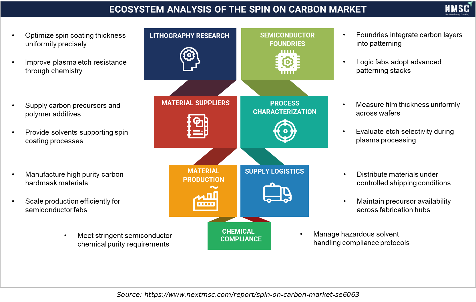
Ecosystem Analysis of the Spin-On Carbon Market

From our research, we found that the Spin-On Carbon Market functions within an ecosystem connecting lithography research, material suppliers, semiconductor foundries, and process characterization teams. Material manufacturers scale high-purity carbon hardmask production, while logistics networks ensure controlled distribution. Ultimately, chemical compliance protocols manage hazardous solvent handling and satisfy stringent semiconductor purity requirements, enabling logic fabs to adopt advanced patterning stacks across the Spin-On Carbon Industry.

Market Drivers & Dynamics

Interactive Dataset
Rising adoption of multi-patterning lithography processes driver +4.6% Global 2026–2035
Expansion of EUV lithography at leading-edge nodes driver +3.8% Asia-Pacific, North America 2026–2033
Growth of 3D NAND and gate-all-around device architectures driver +3.1% Asia-Pacific 2026–2034
Government semiconductor manufacturing incentive programs driver +2.4% North America, Asia-Pacific 2026–2032
Foundry capacity expansion at advanced process nodes driver +2.0% Asia-Pacific, Europe 2026–2035
High cost of advanced-node material qualification restraint −2.2% Global 2026–2030
Concentration risk among a limited supplier base restraint −1.5% Global 2026–2031
Environmental regulation of solvent-based formulations restraint −1.1% Europe 2026–2032
Source: Next Move Strategy Consulting

Growth Drivers

What Is the Primary Growth Driver?

Rising adoption of multi-patterning lithography processes is the primary growth driver, as foundries require multiple hardmask deposition and etch cycles per device layer to achieve sub-10 nm pattern fidelity. We found that continued investment in advanced semiconductor manufacturing is supporting adoption of multi-patterning and related pattern-transfer processes at leading-edge nodes.

How Is EUV Lithography Expansion Driving the Market Growth?

Foundries are rapidly expanding EUV lithography capacity to support leading-edge logic and memory production, directly increasing demand for compatible hardmask and planarization materials. Our assessment indicates that semiconductor-material localization initiatives in South Korea are supporting domestic qualification and supply-chain resilience.

Growth Inhibitors

What Is Restraining the Spin-On Carbon Market?

High cost of advanced-node material qualification remains the primary restraint, as foundries require extensive multi-quarter validation cycles before approving new hardmask formulations for production use. We observed that advanced-node material qualification requires lengthy validation cycles before production approval, slowing supplier diversification.

What Are the Growth Opportunities?

Where Can Next-Generation Etch-Selective Formulations Create Value?

Limited availability of ultra-high etch-selectivity formulations for sub-5 nm patterning creates whitespace for materials vendors able to demonstrate qualified performance at the most advanced nodes. Leading-edge foundries racing to qualify next-generation process technology stand to benefit from early access to differentiated hardmask chemistries.

How Can Regional Manufacturing Capacity Address Supply Concentration?

Persistent supply concentration among a limited global supplier base creates an addressable opportunity for materials producers building regional manufacturing capacity closer to expanding foundry clusters. North American and European foundries pursuing supply-chain diversification are the primary beneficiary segment for regionally qualified capacity.

What Opportunity Exists in Memory-Focused Gap-Fill Chemistry?

Expanding 3D NAND layer counts create a structural opportunity for gap-fill chemistry vendors offering void-free filling performance at increasingly high aspect ratios. Memory-focused integrated device manufacturers scaling next-generation stacking architectures stand to capture yield improvements as advanced gap-fill formulations mature through 2035.

Segmentation Analysis

2025 (USD Million)
2035 (USD Million)
Hardmask 2025: $298.0 Million | 2035: $1,425.0 Million
Hardmask
Planarization 2025: $180.0 Million | 2035: $750.0 Million
Planarizatio
Gap-Fill 2025: $99.0 Million | 2035: $528.0 Million
Gap-Fill
Other Applications 2025: $43.0 Million | 2035: $147.0 Million
Other Applic
Hardmask $298.0 Million $1,425.0 Million 16.94%
Planarization $180.0 Million $750.0 Million 15.34%
Gap-Fill $99.0 Million $528.0 Million 18.22%
Other Applications $43.0 Million $147.0 Million 13.08%

What Is the Outlook Across Spin-On Carbon Applications?

By application, the market spans hardmask, planarization, gap-fill, and other applications such as anti-reflective underlayers. Hardmask dominates with approximately 48% share in 2025, supported by widespread deployment across multi-patterning and EUV process flows. Gap-Fill is the fastest-growing application at 18.22% CAGR, as 3D device architectures increasingly require void-free high-aspect-ratio filling.

2025 (USD Million)
2035 (USD Million)
Below 10 nm
10 to 28 nm
Above 28 nm
Segment Item 2025 (USD Million) 2035 (USD Million) CAGR
Below 10 nm $10.0 USD Million $40.0 USD Million 13.0%
10 to 28 nm $17.1 USD Million $51.1 USD Million 19.0%
Above 28 nm $24.2 USD Million $62.2 USD Million 21.0%

Segment-wise data is locked

Unlock complete segment-wise numbers for By Technology Node.

Unlock Full Data

Which Technology Node Leads Spin-On Carbon Demand?

By technology node, the market is segmented into below 10 nm, 10 to 28 nm, and above 28 nm process categories. Below 10 nm leads with approximately 39% share in 2025, reflecting concentrated foundry investment in leading-edge logic and memory production. Below 10 nm is the fastest-growing technology node at 19.88% CAGR, as foundries accelerate capacity expansion for next-generation process technologies.

2025 (USD Million)
2035 (USD Million)
Foundries
Integrated D
Outsourced S
Segment Item 2025 (USD Million) 2035 (USD Million) CAGR
Foundries $10.0 USD Million $40.0 USD Million 26.0%
Integrated Device Manufacturers $17.1 USD Million $51.1 USD Million 16.0%
Outsourced Semiconductor Assembly and Test $24.2 USD Million $62.2 USD Million 18.0%

Segment-wise data is locked

Unlock complete segment-wise numbers for By End User.

Unlock Full Data

What Is Driving Demand Across End-User Segments?

By end user, the market covers foundries, integrated device manufacturers, and outsourced semiconductor assembly and test providers. Foundries hold approximately 52% share in 2025, driven by concentrated advanced-node production volume among leading pure-play foundry operators. The foundries segment is the fastest-growing end-user segment at 17.35% CAGR, supported by expanding in-house advanced-node capacity among integrated device manufacturers.

2025 (USD Million)
2035 (USD Million)
300 mm
200 mm and B
Segment Item 2025 (USD Million) 2035 (USD Million) CAGR
300 mm $10.0 USD Million $40.0 USD Million 17.0%
200 mm and Below $17.1 USD Million $51.1 USD Million 15.0%

Segment-wise data is locked

Unlock complete segment-wise numbers for By Wafer Size.

Unlock Full Data

Growth Opportunities

Three forward-looking whitespace opportunities stand out for stakeholders positioning ahead of 2035 demand curves.

Where Can Next-Generation Etch-Selective Formulations Create Value?

Limited availability of ultra-high etch-selectivity formulations for sub-5 nm patterning creates whitespace for materials vendors able to demonstrate qualified performance at the most advanced nodes. Leading-edge foundries racing to qualify next-generation process technology stand to benefit from early access to differentiated hardmask chemistries.

How Can Regional Manufacturing Capacity Address Supply Concentration?

Persistent supply concentration among a limited global supplier base creates an addressable opportunity for materials producers building regional manufacturing capacity closer to expanding foundry clusters. North American and European foundries pursuing supply-chain diversification are the primary beneficiary segment for regionally qualified capacity.

What Opportunity Exists in Memory-Focused Gap-Fill Chemistry?

Expanding 3D NAND layer counts create a structural opportunity for gap-fill chemistry vendors offering void-free filling performance at increasingly high aspect ratios. Memory-focused integrated device manufacturers scaling next-generation stacking architectures stand to capture yield improvements as advanced gap-fill formulations mature through 2035.

Regional Outlook

2025 (USD Million)
2035 (USD Million)
North Americ
Europe
Asia-Pacific
Middle East
Latin Americ
Region 2025 (USD Million) 2035 (USD Million) CAGR (%)
North America $10.0 USD Million $40.0 USD Million 9.0%
Europe $17.1 USD Million $51.1 USD Million 27.0%
Asia-Pacific $24.2 USD Million $62.2 USD Million 25.0%
Middle East and Africa $31.3 USD Million $73.3 USD Million 23.0%
Latin America $38.4 USD Million $84.4 USD Million 12.0%

Regional data is locked

Unlock complete regional numbers for this market.

Unlock Full Data

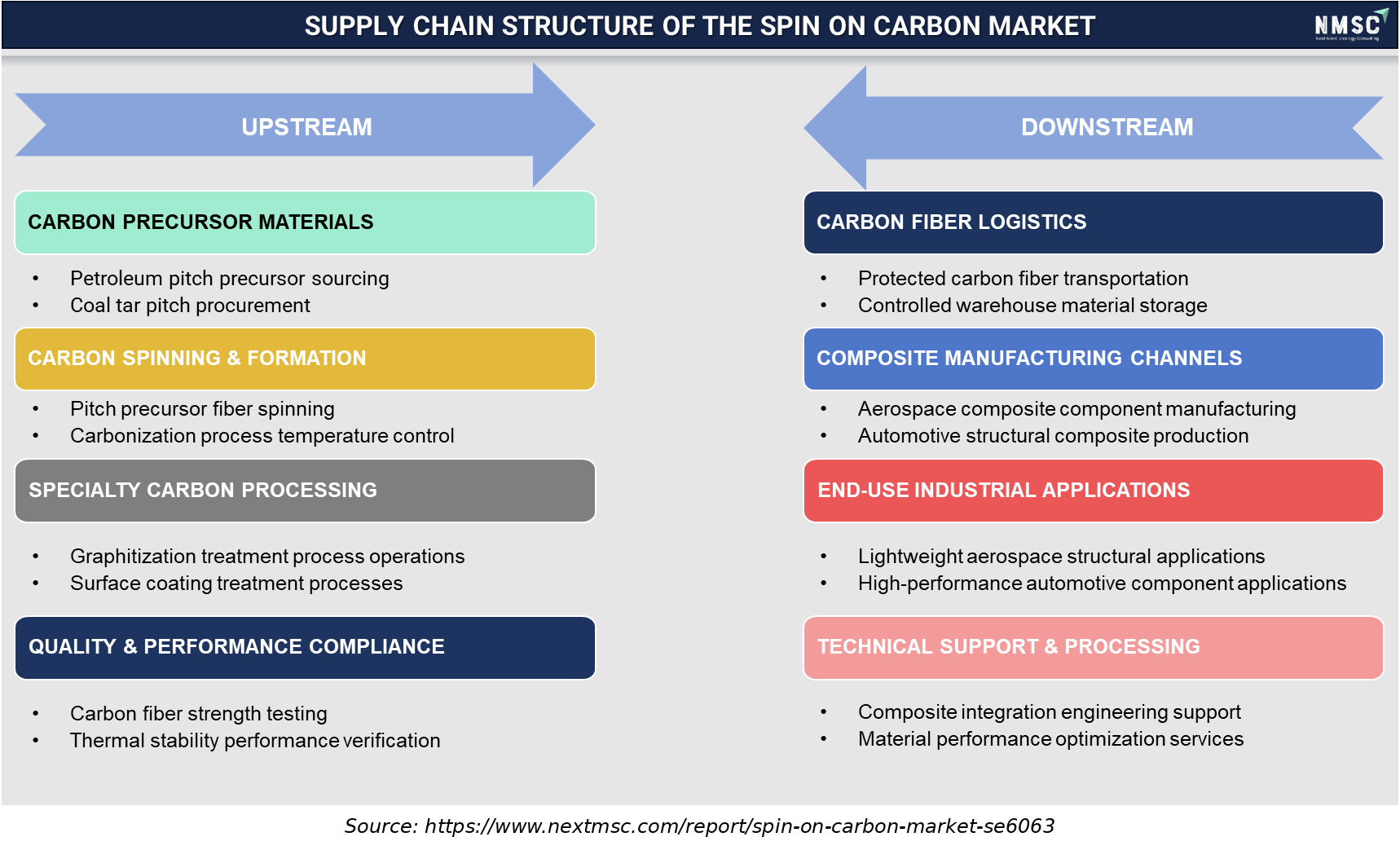
Supply Chain Structure of the Spin-On Carbon Market

Competitive Landscape

Next Move Strategy Consulting's analysis indicates that the competitive landscape remains moderately concentrated, with diversified specialty-chemical suppliers competing alongside dedicated semiconductor-materials producers.

Dimension Description
Market Structure Moderately concentrated, with diversified chemical suppliers and dedicated materials producers coexisting
Innovation Focus High-selectivity hardmask chemistry, gap-fill planarization, EUV-compatible formulations
M&A Activity Selective acquisitions of specialty formulation developers by established materials suppliers

How Do Companies Compete in the Industry?

Companies compete primarily on etch-selectivity performance, qualification speed at advanced nodes, and supply reliability rather than price alone. Diversified specialty-chemical suppliers leverage scale to fund broad formulation portfolios, while focused semiconductor-materials producers differentiate through deep node-specific qualification expertise. Industry participants increasingly publish verifiable performance and reliability data as a core competitive lever across foundry-qualification processes.

Which Competitive Archetypes Dominate the Spin-On Carbon Market?

Two archetypes dominate: diversified specialty-chemical producers extending semiconductor-materials portfolios across multiple product lines, and focused materials developers built around a single differentiated hardmask or gap-fill chemistry. The first archetype competes on breadth and manufacturing scale, while the second competes on technical depth and qualification speed, together defining the industry's competitive structure through 2035.

What Innovation and Differentiation Strategies Are Companies Pursuing?

Companies are investing in high-carbon-content formulations, EUV-compatible hardmask chemistries, and advanced gap-fill materials to differentiate beyond standard planarization products. Innovation focus is shifting from incremental etch-selectivity gains toward engineered multilayer stacks purpose-built for specific patterning schemes, positioning early adopters ahead of tightening foundry qualification requirements across key geographies.

What M&A Activity Is Shaping the Industry?

M&A activity remains selective, concentrated on acquisitions of specialty formulation developers with qualified advanced-node performance by larger materials suppliers seeking rapid portfolio expansion. This pattern reflects broader geographic expansion and pricing strategies aimed at capturing foundry and integrated device manufacturer qualification slots without diluting existing supplier-reliability standards.

Key Market Players

Next Move Strategy Consulting's analysis identifies the following companies as the leading participants shaping the spin-on carbon market through 2035.

JSR Corporation Merck KGaA Brewer Science, Inc. DuPont de Nemours, Inc. Shin-Etsu Chemical Co., Ltd. Tokyo Ohka Kogyo Co., Ltd. Fujifilm Holdings Corporation Sumitomo Chemical Co., Ltd. Dow Inc. Honeywell International Inc. Nissan Chemical Corporation Air Products and Chemicals, Inc. Wacker Chemie AG Kanto Chemical Co., Inc. Samsung SDI Co., Ltd. LG Chem Ltd. Entegris, Inc. Resonac Holdings Corporation Soulbrain Co., Ltd. Dongjin Semichem Co., Ltd.

Latest Developments

Date Event
July 2026 Samsung SDI Co., Ltd. highlighted its Spin-On Hardmask (SOH) technology for semiconductor fabrication, describing spin-coating-based hardmask processes that support etch selectivity and fine-pattern formation for advanced semiconductor architectures.
August 2025 Brewer Science, Inc. announced its “No-Bake Lithography Process” for SEMICON Taiwan 2025, targeting fewer baking steps in lithography stacks containing spin-on carbon, spin-on glass, and photoresist to reduce energy consumption and improve process throughput.
April 2024 Shin-Etsu Chemical Co., Ltd. announced an approximately JPY 83 billion investment in a new semiconductor lithography-materials production and R&D base in Gunma, Japan, expanding capacity for advanced lithography and multilayer materials.

Investment Opportunities

Where Are Capital Inflows Concentrating?

Capital inflows are concentrating in advanced-node hardmask formulation development and regional production-capacity expansion serving leading-edge foundry customers. We found that strategic and institutional investors are prioritizing materials producers with demonstrated foundry qualification track records to reduce commercialization risk, directing capital toward companies with verifiable customer-adoption evidence.

How Is Infrastructure Investment Evolving?

Infrastructure investment is shifting toward regional formulation and blending facilities positioned closer to expanding foundry clusters to reduce supply-chain lead times. Growth in the semiconductor wafer fab equipment market is reinforcing parallel investment in materials-supply infrastructure that overlaps with spin-on carbon demand.

What ESG Considerations Are Shaping Capital Allocation?

Environmental, Social, and Governance considerations are increasingly embedded in capital-allocation screening, with investors requiring transparent solvent-emissions and waste-management disclosures ahead of financing approval. Our findings suggest that this trend is accelerating fastest across Europe, where solvent-emissions disclosure expectations are gaining adoption among institutional chemical-sector investors.

Key Benefits for Stakeholders

How Does This Report Benefit Industry Leaders?

Industry leaders gain access to validated segmentation, regional, and competitive-positioning data that supports formulation-investment prioritization and foundry-qualification planning decisions. The report's forecasts and driver analysis help executive teams benchmark growth trajectories against verified market-sizing methodology ahead of 2035 planning cycles.

How Does This Report Benefit Investors and Financial Analysts?

Investors and financial analysts gain a fundamentals-supported view of market sizing, CAGR drivers, and regional capital-allocation trends, supporting due-diligence and valuation work across semiconductor-materials investment targets. The report's regional and country-level breakdowns help identify underpenetrated markets ahead of broader capital inflows.

How Does This Report Benefit Technology Vendors and Product Teams?

Technology vendors and product teams serving the semiconductor-materials space gain insight into adoption patterns and unmet demand across application and technology-node segments. The report's competitive-landscape and trend analysis inform product-roadmap prioritization for advanced-node qualified formulations through 2035.

Key Market Segments Evaluated

By Application

  • Hardmask
  • Planarization
  • Gap-Fill
  • Other Applications

By Technology Node

  • Below 10 nm
  • 10 to 28 nm
  • Above 28 nm

By End User

  • Foundries
  • Integrated Device Manufacturers
  • Outsourced Semiconductor Assembly and Test

By Wafer Size

  • 300 mm
  • 200 mm and Below

Conclusion & Recommendations

The spin-on carbon market is projected to grow from USD 620.0 Million in 2025 to USD 2,850.0 Million by 2035, reflecting a 16.48% CAGR anchored by expanding multi-patterning and EUV lithography adoption. Long-term outlook remains favorable as foundries qualify higher-selectivity formulations and extend advanced-node capacity across additional geographies through the forecast window.

What Strategic Positioning Do We Recommend?

We recommend that suppliers prioritize advanced-node qualification speed and demonstrated etch-selectivity performance ahead of competitors, given foundry qualification processes increasingly favor suppliers with proven leading-edge track records. Strategic positioning around regional production capacity offers additional differentiation for suppliers serving supply-diversification-focused foundry customers.

How Attractive Is the Market for Investment?

Investment attractiveness remains high, with an absolute dollar opportunity of USD 2,150.0 Million created between 2026 and 2035. Asia-Pacific offers both scale and the highest growth rate at 17.43% CAGR from 2025 to 2035, together presenting a balanced portfolio allocation opportunity for semiconductor-materials investors.

What Market Shifts and Key Risks Should Stakeholders Monitor?

Stakeholders should monitor high qualification costs and supplier-base concentration as the primary risks to sustained growth. A shift toward faster, standardized qualification protocols would accelerate supplier diversification, while unresolved concentration risk could leave foundries exposed to single-supplier dependencies.

What Are the Primary Growth Pathways Through 2035?

Primary growth pathways include expanding high-selectivity formulation development for sub-5 nm patterning, building regional manufacturing capacity to reduce supply concentration, and scaling engineered gap-fill chemistry for advanced memory architectures. Hardmask and Gap-Fill together represent the clearest near-term and long-term growth pathways within the application segmentation.

FAQs

About the Author

Mihul Sharma

Mihul Sharma

Mihul Sharma is Research Associate at Next Move Strategy Consulting, where he has covered technology, industrial, and healthcare markets for 3 years. His work applies structured business research, market analysis, and secondary-source review to assess market trends, competitive developments, and growth opportunities. He supports report development by fully synthesizing industry data, company information, and market signals into concise findings for strategy and investment-focused research teams.

About the Reviewer

Supradip Baul

Supradip Baul

Supradip Baul is an accomplished business consultant and strategist with over a decade of rich experience in market intelligence, strategy, technology, and business transformation. His work has included rigorous qualitative and quantitative analysis across multiple industries, helping clients shape investment decisions and long-term roadmaps. Earlier in his career, he was associated with Gartner, where he contributed to industry-leading reports and market share analyses. He has worked with leading global companies and holds an MBA with a dual specialization in Marketing and Finance.

Download Free Sample

Kishu Kanda

KISHU KANDA

Strategy Analyst

Accenture

We purchased the AI Consumer Market Report from this company. Not only did they customize the report to meet our specific requirements, but they also showed great flexibility in accommodating our budget. The report we received fully met our expectations. Additionally, they provided prompt and thorough responses to both our pre-purchase and follow-up questions. We look forward to working with this company again in the future.

Semih Kavaklioglu

SEMIH KAVAKLIOGLU

Co-Founder & Sales Manager

Decortie

I work a lot in the marketing industry and I know that research is an essential part of any campaign. I have used Market research reports for my own products and I found them to be very informative and well-researched. The team here produces insightful reports for a good price

Kevin Coker

KEVIN COKER

Founder, CEO and Board Diector

Proxima Clinical Research

I have been using Next MSC reports for product positioning in a new geography for a long time. They have by far the best reports I have found and the price is reasonable too!

Rishabh Jogani

RISHABH JOGANI

Strategy Analyst

Accenture Japan

We are incredibly impressed with the market report on the real estate market in India provided by Next Move Strategy Consulting. The report was thorough, insightful, and well-structured, offering deep analysis and actionable recommendations. It not only captured the current trends and dynamics but also provided a forward-looking perspective that has been invaluable for our strategic planning. Their team demonstrated exceptional professionalism, attention to detail, and a profound understanding of the industry. The data-driven insights and clarity of presentation exceeded our expectations, making complex market trends easy to understand. We highly recommend Next Move Strategy Consulting to anyone looking for reliable and comprehensive market research services. Their expertise has given us the confidence to navigate the complexities of the Indian real estate market with clarity and foresight.

Mohit Agarwal

MOHIT AGARWAL

Chief Manager

DryChem India Pvt. Ltd.

Next Move Strategy Consulting is an amazing team of consultants. We required a market study report for our investors on top priority and the team went above and beyond our expectations to deliver the same with ample supporting data within a short time span enabling us to secure the investments and keep our project timeline maintained. Their professionalism, attention to detail, and timely delivery of actionable recommendations have left a lasting impression on our organization.

Custom Market Research Services

We will customize the research for you if the listed report does not fully match your requirements.

Get 30% Free Customization

Select License

This website uses cookies to ensure you get the best experience on our website. Learn more

✖