
Find out How Wafer Handling Robots are Transforming the Semiconductor Industry
Introduction
In the ever-evolving landscape of semiconductor manufacturing, technological innovations continually reshape how industries operate. One such innovation that has garnered significant attention in recent years is the wafer handling robot. These precision machines are transforming the semiconductor industry and beyond, offering unparalleled efficiency and precision in the handling of delicate wafers. This blog explores the capabilities and impact of wafer handling robots.
Enhancing Precision in Semiconductor Manufacturing
Wafer handling robots are instrumental in semiconductor manufacturing, where precision is paramount. These robots are designed to handle semiconductor wafers with the utmost delicacy, ensuring minimal risk of damage or contamination. Their high-precision movements and reliable performance contribute to the production of flawless microchips.
For instance, Kawasaki is a leading provider of wafer handling robots, essential assets in the semiconductor industry, where precision is of utmost importance. These robots play an integral role in the automated manufacture of raw silicon wafers into integrated circuits, and they are renowned for their exceptional precision and speed. They are meticulously crafted to delicately manage semiconductor wafers, offering an unparalleled level of care that minimizes the potential for damage or contamination.
Kawasaki's high-performance specialized handling robots enable manufacturers to automate silicon wafer transfer and logistics throughout the integrated circuit manufacturing process, meeting today's demanding throughput requirements. These robots can handle 300 mm and 450 mm wafers through the production space without damage or disruption, moving wafers from front-opening unified pods (FOUPs) to process tool chambers.
Streamlining Workflow Efficiency
The implementation of wafer handling robots has brought about a transformative shift in manufacturing workflows. These robots, capable of executing repetitive tasks with unparalleled precision and speed, contribute to an enhancement in the overall operational efficiency. This enhancement, in turn, leads to a reduction in production cycle times and a notable increase in throughput, ultimately resulting in substantial cost savings for manufacturers.
KUKA AG showcased its KMR iiwa robot in one of the leading automation trade shows of North America, Automate 2023. KUKA's LBR iiwa 14 R820 CR robot is part of an automated mobile robotic material handling system that can transport 200 mm or 300 mm wafer boxes along with load and unload open cassette machines. This system is designed to allow humans and robots to work together safely and efficiently to move silicon wafers quickly and accurately. The system can automate repetitive tasks, which can save manufacturers time and money by reducing production cycle times and increasing throughput.
Minimizing Contamination Risks
In the quest to streamline workflow efficiency, the focus naturally turns to the critical issue of minimizing contamination risks in semiconductor manufacturing. The industry is acutely aware of how even the tiniest particles can pose a significant threat to the quality and functionality of microchips. It is worth noting that wafer handling robots are vital to this effort, as they operate within meticulously controlled environments. This meticulous control significantly diminishes the risk of contamination, thereby safeguarding the integrity of the wafers at every stage of the production process.
In January 2023, Brooks Automation showcased its collaborative robots lineup PreciseFlex at NEPCON Japan. PreciseFlex collaborative robots are used in automating the loading and unloading of PCB/PCA test fixtures. These systems are designed to operate within meticulously controlled environments, which significantly diminishes the risk of contamination. This, in turn, safeguards the integrity of the wafers at every stage of the production process. Brooks Automation's wafer handling systems are configurable. They can be customized to meet specific application requirements, ensuring that the system is optimized for the specific needs of the semiconductor manufacturing process.
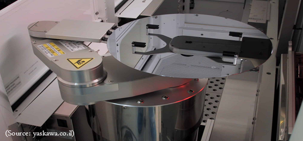
Versatility in Handling
The focus of attention shifts to the remarkable versatility displayed by wafer handling robots when it comes to streamlining workflow efficiency. These robots can effectively manage wafers of diverse sizes and materials, seamlessly adjusting to meet the precise demands of various manufacturing processes. This adaptability and flexibility render them an invaluable asset within semiconductor fabrication facilities.
For instance, Yaskawa Electric launched a wafer handling robot called SEMISTAR-GEKKO MD124D. This robot is a 5-axis single-arm type clean robot designed for transferring semiconductor substrate wafers with improved positioning accuracy. Yaskawa's new SEMISTAR-GEKKO MD124D robot uses a direct drive system to achieve doubled positioning accuracy and 1/6th the vibration of conventional robots. This makes it ideal for transferring 300 mm semiconductor wafers with accuracy and speed, which can help to improve productivity and reduce costs.
Cost-Efficiency and ROI
Cost efficiency and return on investment (ROI) in the context of wafer handling robots are crucial considerations that extend beyond the initial investment. Although the upfront cost of acquiring these robots may appear significant, it is essential to recognize that their true value becomes evident over the long term.
One of the key advantages of wafer handling robots lies in their ability to consistently perform tasks with precision and reliability. This reliability reduces reliance on manual labor, which can be expensive and susceptible to human error. These robots significantly lower operational expenses by automating the delicate and repetitive process of handling semiconductor wafers. This includes reduced labor costs and minimization of costly errors that could result in defective wafers and production delays.
As a result of these cost-saving measures, manufacturers can anticipate a favorable return on their initial investment in wafer handling robots over time. This ROI manifests in several ways, including increased productivity, improved product quality, and reduced production downtime. Moreover, the cost-efficiency achieved through the adoption of these robots can enhance a company's competitive edge in the semiconductor manufacturing industry.
Conclusion
Wafer handling robots have revolutionized manufacturing precision and efficiency in the semiconductor industry. Their ability to enhance accuracy, streamline workflows, minimize contamination risks, and integrate with smart manufacturing systems positions them as indispensable tools in modern production facilities.
As industries continue to evolve, wafer handling robots will likely find applications beyond semiconductors, further cementing their role in shaping the future of manufacturing. Their ability to consistently deliver high-quality results, improve workplace safety, and offer a solid ROI underscores their importance in today's competitive manufacturing landscape.
About the Author
 Shankar Nishant is a researcher at Next Move Strategy Consulting with a cumulative experience of more than four years. Shankar is enthusiastic about new technology, enjoys working with a diverse range of global clients, and has delivered numerous market reports in multiple domains. He can be reached at shankar.dutta@nextmsc.com
Leave a Reply