AI Chips 2025: Huawei, Fujitsu-Nvidia, Microsoft Strategies

Introduction
The global artificial intelligence semiconductor industry has entered a phase of structural transformation, driven by the convergence of generative AI workloads, sovereign technology mandates, and sub-7nm process node commercialization. According to Next Move Strategy Consulting's Artificial Intelligence (AI) Chip Market report, the global AI chip market is projected to reach USD 295.56 billion by 2030, registering a CAGR of 33.2% from 2025 to 2030.
This trajectory reflects a fundamental shift in how enterprises, governments, and hyperscalers procure and deploy compute infrastructure. AI chips — encompassing graphics processing units (GPUs), application-specific integrated circuits (ASICs), neural processing units (NPUs), and field-programmable gate arrays (FPGAs) — have become the critical hardware layer underpinning everything from large language model training to real-time autonomous vehicle inference. The competitive and geopolitical stakes surrounding these components have never been higher, as evidenced by the U.S. government's ongoing effort to establish a global AI chip permit framework that would regulate the flow of advanced accelerators to foreign nations — a development that is simultaneously compressing procurement timelines in allied markets and accelerating domestic chip investment in restricted ones.
For More Information: Download FREE Sample on Artificial Intelligence (AI) Chip Market report
Export Controls, Sovereign Silicon, and the New Architecture of AI Chip Demand
The U.S. Permit Rule Draft: A Market-Reshaping Policy Event
In mid-2026, the U.S. Department of Commerce advanced a draft framework that would require export permits for advanced AI chips shipped to a broad range of countries, moving beyond the existing entity-list approach to a tiered global licensing regime. This regulatory shift has introduced measurable policy risk premiums into AI chip procurement decisions and accelerated foreign governments' urgency to develop sovereign semiconductor capabilities.
The practical consequence for the AI chip market is a bifurcation of demand: U.S.-aligned nations are accelerating purchases of advanced accelerators ahead of potential licensing delays, while nations facing tighter restrictions are channeling investment into domestic alternatives. China's Huawei Ascend series and Cambricon's MLU accelerators have gained renewed procurement attention within China's hyperscaler and state enterprise sectors as a direct result of U.S. export restrictions on leading-edge GPU products. This dynamic does not suppress total AI chip demand — it redirects and, in several cases, amplifies it. Nations that previously relied on imported accelerators are now funding domestic foundry capacity and chip design programs, expanding the total addressable market for AI silicon beyond what a purely commercial demand model would project.
NVIDIA's Rubin Platform and the 2026 Compute Cycle
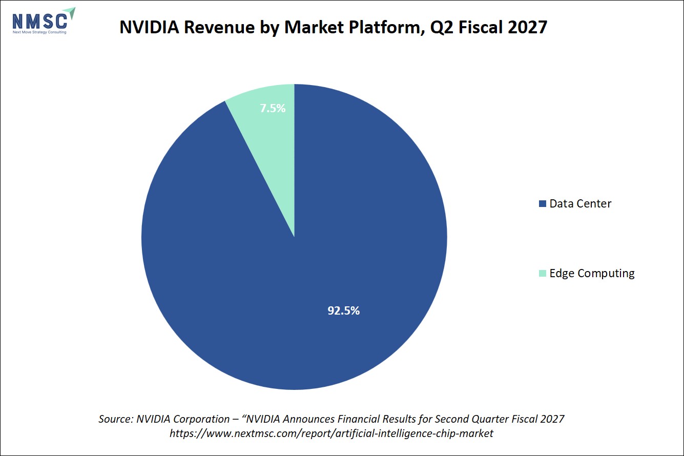
NVIDIA's Rubin GPU architecture, unveiled at COMPUTEX in Taipei and targeting volume shipment in 2026, represents the next generational leap beyond the Blackwell platform. The platform integrates next-generation HBM4 memory and a new NVLink interconnect fabric designed to support rack-scale AI clusters at power envelopes exceeding one megawatt per rack. This introduction has triggered a capital expenditure cycle among hyperscalers — Microsoft, Google, Amazon Web Services, and Meta — each of whom has publicly committed to multi-billion-dollar AI infrastructure investments in 2026.
This hyperscaler-driven demand is structurally different from prior GPU upgrade cycles. Rather than replacing discrete workstation GPUs, these purchases are for purpose-built AI factories: data centers designed from the ground up around GPU cluster density, liquid cooling, and high-bandwidth networking. Each Rubin cluster order therefore represents a multiplier effect on adjacent AI chip categories, including networking ASICs, memory controllers, and inference accelerators.
NMSC Strategic Perspective: The Inference Inflection Point
NextMSC primary research and analysis identifies a critical structural shift occurring within the AI chip market: the center of gravity is moving from training to inference. Through 2024, the majority of AI chip revenue was concentrated in large-scale training clusters — the domain where NVIDIA's H100 and H200 GPUs achieved near-monopoly status. As generative AI applications move from development into production deployment at scale, inference workloads are multiplying at a rate that training workloads cannot match.
This inference inflection has specific implications for chip architecture. Inference workloads favor lower-precision arithmetic (INT8, INT4), higher memory bandwidth relative to compute, and energy efficiency — characteristics that favor custom ASICs and NPUs over general-purpose GPUs. Google's Trillium TPU, AWS's Inferentia2, and a growing cohort of startup inference accelerators from Groq, Cerebras, and SambaNova are each positioned to capture inference spend that would otherwise default to GPU incumbents. The competitive intensity in inference silicon is therefore substantially higher than in training, and the market share distribution across chip types is likely to diversify materially through 2030.
Section Summary: The AI chip market is being reshaped by three simultaneous forces: U.S. export control policy that is redirecting demand and accelerating sovereign chip programs; NVIDIA's Rubin platform triggering a new hyperscaler capital expenditure cycle; and a structural shift from training to inference workloads that is broadening the competitive field beyond GPU incumbents.
Key Takeaways:
-
The U.S. draft AI chip permit framework has introduced policy risk premiums that are accelerating both pre-purchase demand in allied nations and domestic chip investment in restricted markets.
-
NVIDIA's Rubin platform, targeting 2026 volume shipments, is driving a rack-scale AI infrastructure buildout among hyperscalers that amplifies demand across adjacent chip categories.
-
The inference inflection point is diversifying AI chip demand away from GPU-centric training clusters toward custom ASICs and NPUs optimized for energy-efficient, high-throughput inference.
-
Sovereign AI chip programs in China, India, the EU, and Japan are expanding the total addressable market by converting previously import-dependent demand into domestic production investment.
Industry Impact Analysis
Hyperscaler Custom Silicon: Reducing GPU Dependency
The four largest cloud providers — Google, Amazon, Microsoft, and Meta — have each made strategic decisions to develop proprietary AI accelerators rather than rely exclusively on merchant silicon. Google's Trillium chip delivers a 5x performance improvement over its predecessor for data center AI workloads, according to Google's official product announcement. AWS's Trainium2 and Inferentia2 chips, deployed across Amazon SageMaker, enable the company to offer AI training and inference services at cost structures that would be impossible using third-party GPUs at scale.
This vertical integration trend has a dual market impact. On one hand, it reduces the addressable market for merchant GPU vendors within hyperscaler data centers. On the other hand, it validates the economic case for custom AI silicon and has catalyzed broader enterprise interest in application-specific accelerators — expanding the overall market for AI chip design services, EDA tools, and advanced packaging.
Semiconductor Investment and the CHIPS Act Effect
The U.S. CHIPS and Science Act provides chipmakers with USD 39 billion in manufacturing grants plus loans, guarantees, and tax incentives, materially altering the geography of AI chip production. TSMC's Arizona fabs — now producing 4nm chips with 2nm planned — and Intel's Ohio and Arizona expansion represent the first significant onshoring of leading-edge semiconductor manufacturing in the United States in decades.
In Europe, Intel and TSMC have each committed to approximately USD 11 billion in new fab investments in Germany, with the German government co-funding roughly half of each project. These investments are not merely capacity additions; they represent a deliberate restructuring of the global semiconductor supply chain away from geographic concentration in Taiwan and South Korea — a restructuring that directly reduces the supply-side risk premium embedded in AI chip pricing.
According to Deloitte Insights, key semiconductor companies spent approximately USD 300 million on AI tools for chip design in 2023, with that figure projected to reach USD 500 million by 2026. This investment in AI-assisted chip design is compressing development cycles and enabling smaller teams to tape out competitive AI accelerators — a dynamic that is lowering barriers to entry and increasing the number of viable AI chip competitors.
IoT Integration: Expanding the Edge AI Chip Addressable Market
The proliferation of IoT devices is creating a parallel demand vector for AI chips that operates independently of data center dynamics. Connected devices that require on-device AI inference—from industrial sensors performing predictive maintenance to consumer wearables running health-monitoring algorithms—represent an additional source of demand for AI chips beyond hyperscaler procurement.
The edge AI chip segment is architecturally distinct from data center silicon. It prioritizes ultra-low power consumption, small die area, and thermal resilience over raw throughput. Qualcomm's Snapdragon series, MediaTek's Dimensity NPUs, and a growing range of microcontroller-class AI accelerators are competing for this segment, which NMSC's analysis identifies as a structurally high-growth area through 2030.
The broader semiconductor industry remains cyclical, while the adoption of AI across data centers, industrial applications, and connected devices continues to shape demand for specialized computing hardware. The expansion of edge AI creates opportunities for chip designers to develop energy-efficient solutions tailored to application-specific workloads.
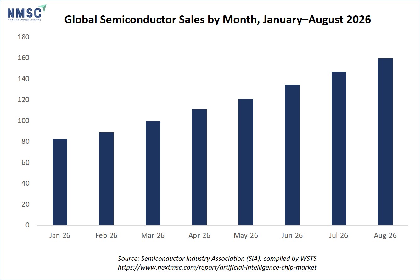
Section Summary: The AI chip industry is experiencing simultaneous demand expansion across data center, edge, and sovereign segments, while supply-side investment through the CHIPS Act and European fab programs is reducing geographic concentration risk. Hyperscaler custom silicon is reshaping competitive dynamics without suppressing total market growth.
Key Takeaways:
-
Google's Trillium, AWS Trainium2/Inferentia2, and equivalent hyperscaler custom chips are reducing merchant GPU dependency within cloud data centers while validating the broader custom silicon market.
-
The U.S. CHIPS Act's USD 39 billion in manufacturing grants is funding the first significant onshoring of leading-edge AI chip production in the United States.
-
Deloitte Insights projects semiconductor companies' AI-assisted chip design spending to reach USD 500 million by 2026, compressing development cycles and lowering barriers to entry.
-
IoT ecosystem spending exceeding USD 1 trillion by 2026 is creating a structurally distinct edge AI chip demand vector that operates independently of data center procurement cycles.
Pros and Cons of Recent Market Developments
|
Recent Development |
Pros |
Cons |
|
U.S. AI Chip Export Permit Framework |
Accelerates pre-purchase demand in allied nations; incentivizes domestic chip investment globally; reduces long-term supply concentration risk |
Introduces procurement uncertainty; may delay AI adoption in developing markets; risks fragmenting the global semiconductor supply chain |
|
NVIDIA Rubin Platform Launch (2026) |
Delivers step-change performance for LLM training and inference; drives hyperscaler capex cycle; stimulates adjacent chip demand (networking, memory, packaging) |
Concentrates market power further in a single vendor; high power consumption per rack raises data center energy costs; supply constraints likely in initial ramp |
|
Hyperscaler Custom Silicon (Google Trillium, AWS Trainium2/Inferentia2) |
Reduces cloud AI service costs; validates custom ASIC economics; stimulates enterprise interest in application-specific accelerators |
Reduces addressable market for merchant GPU vendors within hyperscaler data centers; requires significant upfront R&D investment |
|
CHIPS Act Manufacturing Investments (USD 39Bn, U.S.) |
Reduces geographic supply concentration; creates domestic high-skill employment; lowers long-term supply-side risk premiums |
Multi-year construction timelines mean near-term supply relief is limited; government co-funding creates subsidy dependency risks |
|
2nm Process Node Commercialization (TSMC N2) |
Delivers ~15-20% performance improvement and significant power reduction vs. 3nm; enables next-generation AI chip architectures |
Extremely high capital cost per wafer; limited initial production capacity; yield ramp uncertainty in early production phases |
|
Sovereign AI Chip Programs (China, India, EU, Japan) |
Expands total addressable market; reduces single-vendor dependency; stimulates global semiconductor R&D investment |
Domestic chips often lag leading-edge performance by 1-2 generations; risk of market fragmentation and incompatible software ecosystems |
Key Data & Statistics
|
Industry Vertical |
AI Adoption Maturity Rate (Near-Term, 3+ Years) |
|
Retail |
54% |
|
Technology, Communications & Entertainment |
47% |
|
Financial Services |
41% |
|
Healthcare |
37% |
|
Automotive |
35% |
Future Outlook & Forecast
The Path to USD 295.56 Billion: Structural Demand Drivers Through 2030
NextMSC primary research and analysis projects the global AI chip market to reach USD 295.56 billion by 2030, growing at a CAGR of 33.2% from 2025. This trajectory is underpinned by three structural demand drivers that are specific to the AI chip market and cannot be replicated by substituting a different technology category.
First, the generative AI infrastructure buildout has no historical precedent in terms of capital intensity per unit of compute. Training a frontier large language model requires clusters of thousands of high-end GPUs operating continuously for weeks or months. As model complexity increases — from hundreds of billions to trillions of parameters — the compute requirement scales super-linearly, meaning each new model generation requires disproportionately more AI chip capacity than its predecessor. This dynamic ensures that even if the number of frontier AI labs remains constant, their aggregate chip demand will continue to grow at rates that outpace general semiconductor market growth.
Second, the inference deployment wave is only beginning. As of 2026, the majority of generative AI applications are still in early commercial deployment. The transition from pilot to production — across healthcare diagnostics, financial services automation, autonomous vehicles, and industrial robotics — will require inference infrastructure at a scale that dwarfs current training cluster investments. NMSC's analysis of the inference segment identifies it as the primary volume driver for AI chip unit shipments through 2030, even as training clusters continue to dominate revenue per unit.
Third, the 2nm process node transition will reset performance benchmarks and stimulate a hardware refresh cycle. TSMC's N2 process, which entered mass production in 2025, delivers approximately 15-20% performance improvement and meaningful power reduction compared to 3nm. For AI chip designers, this translates directly into higher throughput per watt — the metric that determines data center operating economics. As 2nm-based AI chips reach volume availability through 2026-2027, they will trigger a replacement cycle among hyperscalers and enterprise AI infrastructure operators who purchased 5nm and 7nm-based accelerators in 2023-2024.
Regional Outlook
Asia-Pacific maintains the largest share of the global AI chip market, anchored by TSMC's foundry dominance in Taiwan, Samsung's and SK Hynix's HBM memory leadership in South Korea, and China's rapidly expanding domestic AI chip ecosystem. According to the Economist Intelligence Unit (EIU), Malaysia has also increased its participation in chip production, attracting capital from global chip-producing companies — with Infineon Technologies AG planning a USD 5.8 billion investment in a third chip testing facility in the country.
North America is the fastest-growing region, driven by hyperscaler capital expenditure, the CHIPS Act manufacturing buildout, and the concentration of frontier AI research and development in the United States and Canada. The Canadian government's commitment of USD 1.46 billion to AI infrastructure — specifically to expand domestic data center capacity for AI researchers and developers — reflects a broader pattern of government-led AI chip demand creation that NMSC's analysis identifies as a structural market driver across G7 nations.
Section Summary: The AI chip market's path to USD 295.56 billion by 2030 is supported by three non-substitutable demand drivers: the capital-intensive generative AI training buildout, the emerging inference deployment wave, and the 2nm process node refresh cycle. Regional growth is led by Asia-Pacific in volume and North America in growth rate.
Key Takeaways:
-
Frontier LLM training compute requirements scale super-linearly with model complexity, ensuring sustained AI chip demand growth independent of the number of AI labs.
-
The inference deployment wave — as generative AI moves from pilot to production across healthcare, finance, automotive, and industrial sectors — will drive AI chip unit volume growth through 2030.
-
TSMC's 2nm process node, in mass production since 2025, will trigger a hardware refresh cycle among hyperscalers and enterprise AI operators through 2026-2027.
-
Government-led AI infrastructure investment across G7 nations — including Canada's USD 1.46 billion commitment — is creating a structural public-sector demand layer that supplements commercial hyperscaler procurement.
Next Steps for Stakeholders
For C-Level Executives and Technology Leaders:
-
Audit AI chip procurement exposure to export control risk. Organizations with AI infrastructure in jurisdictions subject to U.S. export licensing requirements should conduct a supply chain risk assessment and identify alternative accelerator options — including domestic or allied-nation alternatives — before licensing delays materialize.
-
Evaluate the inference-to-training ratio of your AI workload portfolio. If your organization's AI deployment is shifting from model development to production inference, the optimal chip architecture may differ significantly from your current GPU-centric infrastructure. Custom ASICs and NPUs from hyperscaler cloud providers or specialized inference vendors may deliver superior cost-per-inference economics at scale.
-
Engage with CHIPS Act and equivalent national semiconductor programs. Organizations with manufacturing operations in the United States, Germany, or other jurisdictions with active semiconductor investment programs should assess eligibility for grants, tax incentives, and co-investment opportunities that can materially reduce AI infrastructure capital costs.
-
Plan hardware refresh cycles around the 2nm availability window. TSMC's N2 process is ramping through 2026-2027. Organizations planning major AI infrastructure investments should model the total cost of ownership implications of purchasing 3nm-based accelerators now versus waiting for 2nm-based alternatives, factoring in the performance-per-watt improvements and their impact on data center operating expenses.
For Institutional Investors:
-
Differentiate between training-focused and inference-focused AI chip vendors. The inference inflection point creates asymmetric growth opportunities for companies with architectures optimized for low-precision, high-throughput inference — a segment where GPU incumbents' dominance is less entrenched than in training.
-
Assess sovereign AI chip program investment opportunities. Government-backed domestic chip programs in India, the EU, Japan, and Southeast Asia represent early-stage investment opportunities in markets where import substitution is a policy imperative rather than a commercial preference.
-
Evaluate advanced packaging and HBM memory as AI chip adjacencies. The performance of AI accelerators is increasingly constrained by memory bandwidth rather than compute density. Companies providing high-bandwidth memory (HBM), advanced packaging (CoWoS, SoIC), and chiplet interconnect solutions are structurally positioned to benefit from AI chip demand growth regardless of which GPU or ASIC vendor wins market share.
Conclusion
The global AI chip market is at an inflection point where technology, geopolitics, and capital are converging to reshape the semiconductor industry's competitive structure. NextMSC primary research and analysis projects the market to grow from USD 52.92 billion in 2024 to USD 295.56 billion by 2030 at a 33.2% CAGR — a trajectory that reflects not a single demand driver but a compounding of generative AI infrastructure investment, inference deployment at scale, sovereign chip programs, and process node transitions.
The U.S. export permit framework, NVIDIA's Rubin platform, and TSMC's 2nm ramp are not isolated events; they are interconnected signals of a market that is simultaneously expanding in total size and diversifying in competitive structure. For executives and investors, the strategic imperative is to move beyond GPU-centric thinking and develop a nuanced understanding of how training, inference, edge, and sovereign AI chip segments will evolve at different rates and under different competitive dynamics through 2030. Organizations that map their AI chip strategy to these structural shifts — rather than to the last cycle's vendor relationships — will be best positioned to capture the performance and cost advantages that the next generation of AI silicon will deliver.
About the Author
 Sanyukta Deb
— Sanyukta Deb is Digital Marketing Team Lead at Next Move Strategy Consulting, where she has led content strategy and technical SEO for the firm's B2B market research publications for over 2 years. Her editorial process translates NextMSC's primary and secondary research — spanning technology, industrial, and consumer sectors — into commercial narratives, backed by search-intent, keyword, and competitive analysis. She brings 5 years of overall experience in digital marketing and content strategy.
About the Reviewer
 Debashree Dey
— Debashree Dey is Assistant Manager at Next Move Strategy Consulting, where she supports cross-vertical market content and communications across diverse industries for 6 years. Her professional background includes senior content writing, communications, and published manuscript authorship, with experience developing audience-focused business narratives and maintaining clear, consistent messaging. Her role supports research-led content development and editorial quality across NextMSC publications.
















Add Comment