Semiconductor Recycling Market By Feedstock Source {Wafer Reclaim (Prime Wafers, Test Wafers, and Others), Fab Scrap, Assembly Scrap, Facility Scrap}, By Recovered Output {Reclaimed Wafers (Silicon, SiC, and Others),Chemicals, Parts}, By Processing Route (Mechanical, Chemical, Thermal, Electrochemical, Membrane, Direct Reclaim), and By Commercial Model {Tolling (Fee for Service, Treatment Contracts), Merchant (Scrap Purchase, Resale), Hybrid} – Global Analysis & Forecast, 2025–2035
Industry: Semiconductor & Electronics | Publishing Date: June 6, 2026 | Last Updated: September 30, 2026 | No of Pages: N/A | No. of Tables: N/A | No. of Figures: N/A | Format: PDF | Report Code: SE4611
Industry Outlook
The global Semiconductor Recycling Market size was valued at USD 18.57 billion in 2025 and is expected to be valued at USD 21.44 billion by the end of 2026. The industry is projected to grow, hitting USD 77.20 billion by 2035, with a CAGR of 15.2% between 2026 and 2035.
Semiconductor Recycling Market Size & Forecast
|
Parameters |
Details |
|
Market Size in 2026 |
USD 21.44 Billion |
|
Revenue Forecast in 2035 |
USD 77.20 Billion |
|
Growth Rate |
CAGR of 15.2% from 2026 to 2035 |
|
Analysis Period |
2025–2035 |
|
Base Year Considered |
2025 |
|
Forecast Period |
2026–2035 |
|
Market Size Estimation |
Billion (USD) |
|
Companies Profiled |
20 |
|
Countries Covered |
33 |
|
Market Share |
Available for 10 companies |
Based on NMSC’s primary research, we observed that the global semiconductor recycling market is gaining significant traction, supported by rising semiconductor production volumes, increasing costs of high-purity raw materials, and a stronger industry-wide push toward sustainability. Companies integrate wafer reclaim, metal recovery, and scrap recycling into fabrication workflows, thereby reducing dependence on virgin silicon and precious metals while improving cost efficiency. At the same time, growing process complexity in advanced nodes increases material wastage, which further strengthens the need for efficient recycling solutions. Consequently, advancements in precision polishing, chemical treatment, and contamination removal improve wafer usability and recovery rates, enabling multiple reuse cycles and reinforcing circular manufacturing practices across fabs.
Moreover, based on our regional evaluation across Asia-Pacific, North America, and Europe, we noticed that adoption trends vary significantly depending on regulatory frameworks, industrial maturity, and semiconductor manufacturing concentration. Asia-Pacific leads the market due to its dominant semiconductor production base, cost-sensitive manufacturing environment, and well-established recycling ecosystems. Meanwhile, North America benefits from advanced recycling technologies, strict environmental compliance requirements, and strong collaboration between fabs and recycling partners. In contrast, Europe places greater emphasis on circular economy mandates and sustainability-driven policies, which accelerate structured recycling initiatives. Emerging markets such as India and Southeast Asia show increasing adoption, supported by expanding electronics manufacturing, rising e-waste volumes, and gradual regulatory tightening.
Additionally, we identified that operational efficiency, recovery yield, and material purity remain key competitive differentiators in the semiconductor recycling market. Companies such as Pure Wafer, RS Technologies, TES-AMM, and Umicore highlight a strong focus on enhancing process automation, improving extraction efficiency, and scaling recycling capacities to meet growing demand. Furthermore, these companies invest in advanced separation technologies and closed-loop recycling systems to achieve higher purity levels suitable for semiconductor-grade applications. As a result, improved recovery economics, reduced processing time, and consistent material quality strengthen supply chain resilience while supporting long-term sustainability and cost optimization objectives across the semiconductor value chain.
What Are the Key Trends in the Semiconductor Recycling Industry?
How Is “Chiplet-to-Chiplet” Circularity Redefining Semiconductor Recycling?
Based on our analysis of next-generation semiconductor architectures, we observed that the shift toward chiplet-based designs is fundamentally transforming recycling practices beyond conventional material recovery. Our interactions with advanced packaging engineers and AI hardware manufacturers indicate that heterogeneous de-manufacturing is gaining traction, wherein functional chiplets are selectively extracted from high-value components such as GPUs and AI accelerators. In contrast to traditional recycling, which focuses on bulk material extraction, this approach enables the preservation of compute-ready units through AI-driven precision robotics and intelligent disassembly systems. Furthermore, recovered chiplets are increasingly repurposed in secondary applications, including edge computing and embedded systems, thereby extending component lifecycles and reducing overall system costs. As a result, with growing chiplet standardization, this model reinforces circular design principles while unlocking new value streams within semiconductor recycling ecosystems.
How Is SiC and GaN Specialization Shaping High-Value Material Recovery?
From our market assessments focused on power electronics and advanced materials, we determined that the rise of wide-bandgap semiconductors is driving a new wave of specialized recycling capabilities. Through our engagements with power device manufacturers and materials processing companies, we identified that Silicon Carbide (SiC) and Gallium Nitride (GaN) substrates require highly controlled recovery processes due to their structural complexity and high economic value. Compared to traditional silicon recycling, these materials demand precision separation, contamination control, and advanced thermal and chemical treatments to retain usability. At the same time, industry developments indicate the emergence of dedicated recovery lines tailored for WBG materials, particularly aligned with the rapid expansion of electric vehicles and renewable energy systems. Consequently, as demand for SiC and GaN accelerates, specialized recycling improves recovery efficiency while strengthening material supply security for next-generation power electronics.
How Are Real-Time “Waste-to-Wafer” Analytics Enhancing Traceability and Sustainability?
Based on our evaluation of digital integration across semiconductor value chains, we observed that real-time analytics is redefining transparency in recycling operations. Insights gathered from fab sustainability teams and digital infrastructure providers indicate that blockchain frameworks and IoT-enabled tracking systems are increasingly embedded within scrap management processes to ensure end-to-end traceability of recycled materials. In parallel, these systems capture granular data on material origin, processing stages, and recovery outputs, enabling manufacturers to quantify and validate the proportion of recycled content in newly fabricated wafers. Moreover, such “waste-to-wafer” visibility supports compliance with evolving sustainability reporting standards while strengthening confidence in green manufacturing practices. Ultimately, as digital traceability becomes more standardized, this integration enhances accountability, improves resource optimization, and establishes a scalable pathway toward fully circular semiconductor production.
Ecosystem Analysis of the Semiconductor Recycling Market
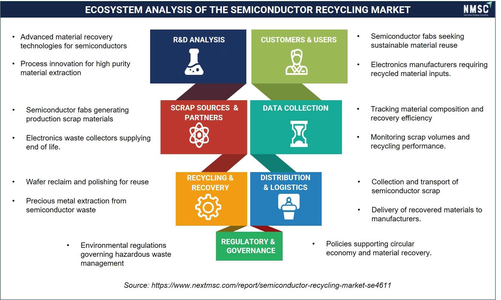
Based on industry observations and policy developments, we found that the semiconductor recycling market ecosystem operates through a structured network of fabs, recyclers, and regulators. We identified that scrap generation from fabrication facilities, combined with advanced recovery technologies, enables efficient extraction of high-purity materials. Furthermore, data-driven tracking improves yield optimization and traceability. Regulatory frameworks such as circular economy mandates reinforce compliance and material recovery practices. As a result, this integrated ecosystem supports sustainable supply chains while addressing critical material dependencies across global semiconductor manufacturing.
What Are the Key Market Drivers, Breakthroughs, and Investment Opportunities that will Shape the Semiconductor Recycling Market in the Next Decade?
Growth Catalyst & Risk Assessment Matrix
|
Drivers / Trends / Restraints |
(+/–) % Impact On CAGR Forecast |
Geographic Relevance |
Impact Timeline |
|
Rising AI-driven semiconductor demand increasing dependence on recycled rare earths, gallium, and precious metals |
+1.3% |
Global; strongest in North America, China, and South Korea |
Short to medium term (1–3 years) |
|
Government initiatives supporting material sovereignty and domestic semiconductor recycling infrastructure development |
+1.1% |
North America, Europe, India, and emerging Southeast Asian markets |
Short to medium term (1–3 years) |
|
Transition toward chiplet architectures and component-level reuse strengthening chiplet circularity practices |
+0.9% |
North America, Taiwan, and South Korea |
Medium term (2–4 years) |
|
Increasing adoption of SiC and GaN semiconductor recycling driven by EV and renewable energy expansion |
+0.8% |
China, Europe, Japan, and North America |
Medium term (2–4 years) |
|
Integration of digital traceability technologies, including IoT-enabled monitoring and blockchain-based tracking systems, improving “waste-to-wafer” transparency |
+0.6% |
Global; strongest in Europe and North America |
Medium term (2–4 years) |
|
Increasing technical complexity of advanced semiconductor nodes limiting high-purity material recovery efficiency |
–1.0% |
Global; strongest impact in Taiwan, South Korea, and North America |
Medium to long term (3–5 years) |
Based on our evaluation of global semiconductor value chain dynamics, we identified that the semiconductor recycling market is gaining strong momentum, driven primarily by rising material costs, increasing semiconductor production volumes, and growing sustainability mandates. Our interactions with semiconductor manufacturers and recycling service providers show that recycling is increasingly adopted as a strategic approach to reduce dependence on virgin raw materials and stabilize long-term procurement costs. Advancements in precision recovery technologies, chemical processing, and automated disassembly expand recycling capabilities, enabling efficient extraction of high-purity silicon, precious metals, and specialty materials from complex semiconductor waste streams. However, our assessment also indicates that technical complexity associated with advanced nodes and high capital investment requirements constrain large-scale adoption, particularly for high-end semiconductor applications. At the same time, the emergence of closed-loop recycling models and Recycling-as-a-Service (RaaS) frameworks creates new growth opportunities by improving material traceability, optimizing resource utilization, and supporting scalable circular manufacturing ecosystems.
Growth Drivers:
How Is AI-Induced Material Scarcity Accelerating Semiconductor Recycling Adoption?
Based on our analysis of semiconductor demand patterns, we identified that the rapid expansion of AI-driven workloads is intensifying pressure on the availability of high-purity materials. Interactions with AI chip designers and data center operators indicate that advanced processors increasingly rely on scarce elements such as gallium, palladium, and rare earth metals, thereby creating supply imbalances across global value chains. According to the Semiconductor Industry Association (SIA), global semiconductor sales reached USD 75.3 billion in November 2025, marking a 29.8% increase from USD 58.0 billion in November 2024. We observed that rising AI-driven semiconductor demand is increasing the need for semiconductor recycling and material recovery. This massive year-on-year growth underscores the accelerating demand for high-end chips, which is a primary driver for secondary material recovery through recycling. As AI chips account for a growing share of industry revenue, material consumption scales disproportionately, further tightening supply conditions. In response, urban mining, particularly the recovery of materials from decommissioned servers and legacy data center infrastructure gains economic viability compared to traditional mining. Consequently, recycling transitions from a sustainability initiative to a cost-competitive sourcing strategy, strengthening its role as a primary supply channel for critical semiconductor materials.
How Is Geopolitical De-Risking Driving Domestic Semiconductor Recycling Investments?
From our evaluation of policy frameworks and supply chain strategies, we determined that governments are increasingly positioning semiconductor recycling as a strategic lever for material sovereignty. As of 2026, under the EU Critical Raw Materials Act, the European Union has set a target to meet 25% of its strategic raw material demand through recycling by 2030, positioning domestic recycling as a key pillar of material sovereignty and reduced import dependency. Further, Engagements with national policymakers and semiconductor supply chain planners reveal that reliance on geographically concentrated raw material sources is prompting large-scale investments in domestic recycling infrastructure. Programs across the United States, Europe, and India prioritize the development of localized recycling hubs through subsidies, incentives, and regulatory support, aligned with broader “resilient supply chain” mandates. At the same time, these initiatives encourage closer integration between fabrication facilities and recycling ecosystems to ensure secure material loops. As a result, recycling evolves into a critical component of national semiconductor strategies, reinforcing supply security while supporting long-term industrial resilience.
Growth Inhibitor:
How Is Advanced Node Complexity Restricting Semiconductor Recycling Scalability?
Based on our assessment of next-generation semiconductor architectures, we noticed that shrinking process nodes are creating fundamental barriers to effective material recovery. Our discussions with process engineers and materials scientists indicate that advanced semiconductor devices increasingly incorporate highly complex, multi-layered architectures with heterogeneous material integration within compact nanoscale structures. Unlike earlier generations, where separation processes remain relatively standardized, these advanced semiconductor designs require extremely precise and energy-intensive extraction techniques. According to the United Nations Department of Economic and Social Affairs (UNDESA) in 2025, recycling potential for critical materials such as cobalt, lithium, and rare earth elements remains below 5% due to technological and material recovery limitations. Consequently, conventional chemical and mechanical recycling methods struggle to isolate usable materials without contamination or reduction in material purity. In addition, the energy and cost required to separate these nanoscale material stacks often exceed the economic value of the recovered output, thereby limiting commercial viability. As a result, advanced node complexity continues restricting large-scale adoption of semiconductor recycling solutions across cutting-edge semiconductor applications.
Growth Opportunity:
How Are Closed-Loop Foundry Models Creating New Semiconductor Recycling Market Opportunities?
From our market evaluation of emerging service models, we determined that closed-loop recycling frameworks are redefining value creation across the semiconductor ecosystem. Our Interactions with foundry operators and fabless semiconductor companies indicate that Recycling-as-a-Service (RaaS) models are gaining traction, wherein clients return production scrap and end-of-life components in exchange for incentives on future manufacturing capacity. This approach integrates recycling directly into the foundry value chain, enabling a seamless “waste-to-wafer” cycle that enhances resource efficiency. In February 2026, the Government of India announced India Semiconductor Mission (ISM) 2.0 to strengthen semiconductor equipment, materials, and supply chain capabilities. We observed that expanding semiconductor infrastructure is creating opportunities for semiconductor recycling and material recovery activities. Furthermore, such models allow manufacturers to quantify and utilize recycled content within their production pipelines, aligning with sustainability targets and cost optimization strategies. As adoption scales, closed-loop systems position recycling not only as a recovery mechanism but as a strategic asset, transforming waste into a tradable input within semiconductor manufacturing ecosystems.
Supply Chain Structure of the Semiconductor Recycling Market
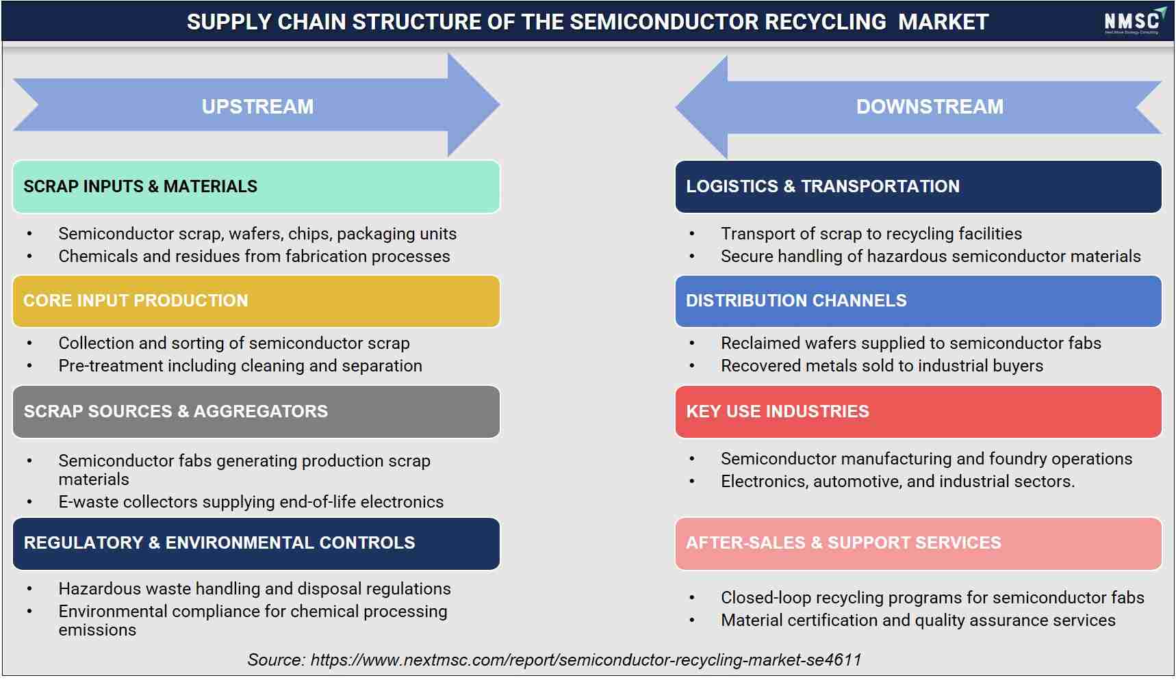
From our evaluation of semiconductor value chains, we found that recycling supply chains are designed to efficiently convert waste into reusable materials. Upstream activities involve structured collection and pre-treatment of scrap from fabs and electronic waste streams. These materials undergo specialized recovery and refining processes to meet high purity standards. Subsequently, downstream logistics ensure secure transport and reintegration into manufacturing cycles. Additionally, closed-loop recycling models are increasingly adopted by leading fabs. Therefore, this supply chain enhances resource efficiency while strengthening material security and operational resilience.
How Is the Semiconductor Recycling Market Segmented in This Report, And What Are the Key Insights from the Segmentation Analysis?
Market Highlights & Strategic Insights – Semiconductor Recycling Market:
|
Segments |
Key Takeaways |
|
Feedstock Source |
Fab scrap dominates the Semiconductor Recycling market share, driven by continuous generation of wafer rejects, CMP slurry, and spent chemicals in high-volume fabs. Wafer reclaim remains a key segment due to repeated reuse of test and dummy wafers in production cycles. Assembly scrap gains traction with increasing substrate and packaging complexity, while facility scrap maintains steady demand from periodic replacement of quartzware and filtration systems. R&D and other scrap contribute limited but consistent volumes linked to pilot production and innovation activities. |
|
Recovered Output |
Metals lead the semiconductor recycling market, supported by the high recovery value of precious metals such as gold, palladium, and silver from semiconductor waste. Reclaimed wafers follow, driven by demand for cost-efficient silicon reuse in testing and fabrication. Chemicals gain importance as fabs increasingly recover acids and solvents, while parts such as photomasks and quartzware support refurbishment and reuse cycles. |
|
Processing Route |
Chemical processing dominates, as it enables high-purity extraction required for semiconductor-grade materials. Mechanical processes support pre-treatment and separation, while thermal methods are used for recovery from complex waste streams. Electrochemical and membrane processes are applied in precision recovery and filtration, while direct reclaim supports wafer reuse with minimal reprocessing. |
|
Commercial Model |
The merchant model dominates, driven by strong demand for recovered materials and active resale markets. Tolling model remains significant, as fabs outsource recycling under fee-based contracts. Hybrid models are gaining traction by combining processing services with material resale, improving overall value capture. |
By Feedstock Source Insights
Which Feedstock Sources Drive the Semiconductor Recycling Market Growth?
Based on our feedstock-level analysis of semiconductor recycling operations, we observed that the semiconductor recycling market is segmented into wafer reclaim, fab scrap, assembly scrap, facility scrap and R&D scrap.
From our evaluation of recycling flows across semiconductor fabrication environments, we found that fab scrap drives market growth, as it is continuously generated through wafer rejects, CMP slurry, and spent chemicals in high-volume production. In contrast, wafer reclaim remains a foundational segment, since test and dummy wafers are repeatedly reused within fabrication cycles. Furthermore, our interactions with process engineers indicate that assembly scrap is gaining traction, driven by increasing packaging complexity and substrate usage, while facility scrap maintains steady demand due to periodic replacement of quartzware and filtration systems. Meanwhile, R&D contribute niche but consistent volumes, reflecting ongoing pilot-scale production and innovation activities. As a result, feedstock streams are becoming more structured, enabling recyclers to plan recovery processes and scale operations more efficiently.
By Recovered Output Insights
How Do Recovered Outputs Influence Value Creation in the Semiconductor Recycling Market?
Based on our detailed assessment of recovered material streams, we noticed that the semiconductor recycling market is segmented into reclaimed wafers, metals, chemicals, parts, and other outputs.
From our analysis of recovery economics, we found that metals lead value creation, as precious metals such as gold, palladium, and silver offer high recovery value. At the same time, reclaimed wafers remain a key segment, supported by demand for cost-efficient silicon reuse in testing and fabrication processes. Moreover, our interactions with recycling operators indicate that chemicals, including acids and solvents, are increasingly recovered, thereby reducing operational costs and improving resource efficiency. In addition, parts such as photomasks and quartzware support refurbishment cycles, while other outputs continue to expand gradually as recyclers explore additional value streams. Consequently, diversified output recovery strengthens revenue streams and enhances overall economic viability.

By Commercial Model Insights
How Do Commercial Models Shape Revenue Generation in the Semiconductor Recycling Market?
Based on our evaluation of industry business models, we observed that the semiconductor recycling market is segmented into merchant, tolling, and hybrid models.
From our analysis of transaction structures and value flows, we found that the merchant model drives revenue generation, as recyclers purchase semiconductor scrap and monetize recovered materials through resale. Meanwhile, the tolling model remains widely adopted, enabling semiconductor manufacturers to outsource recycling under fee-based agreements while retaining material ownership. Furthermore, our interactions with industry participants indicate that hybrid models are gaining traction, as they combine processing services with material resale to maximize value capture. As a result, evolving commercial models improve profitability, increase flexibility, and strengthen long-term value chain integration.

Regional Outlook:
Geographic Performance Snapshot:
|
Region |
Key Takeaways |
|
North America |
A significant market for semiconductor recycling, driven by demand from automotive electronics, renewable energy systems, and advanced manufacturing. Growth is supported by supply chain security initiatives, domestic semiconductor processing investments, and increasing focus on circular economy practices and critical material recovery. |
|
Europe |
Strong focus on sustainability and circular economy policies drives semiconductor recycling adoption. Strict environmental regulations and carbon-reduction targets encourage recycling of electronic materials. Growth is supported by industrial recycling initiatives in automotive, industrial, and electronics sectors, along with investments in green manufacturing technologies. |
|
Asia-Pacific |
The leading region in semiconductor production and recycling activity due to large-scale electronics manufacturing in China, Japan, South Korea, and India. High production volumes of semiconductors and electronics generate significant recycling demand. Rapid industrialization, urbanization, and strong supply chain ecosystems further strengthen the region’s dominance. |
|
Latin America |
An emerging market with gradual development in semiconductor recycling. Growth is driven by infrastructure expansion, increasing electronics consumption, and improving awareness of e-waste management. Recycling systems and material recovery capabilities are still developing but steadily improving. |
|
Middle East & Africa |
Developing region in semiconductor recycling, supported by infrastructure growth and rising electronic waste generation. The Middle East is investing in industrial diversification and downstream material recovery, while Africa is gradually improving waste processing and recycling infrastructure. |
The semiconductor recycling market is geographically studied across North America, Europe, Asia Pacific, Latin America and Middle East & Africa and each region is further studied across countries.
Semiconductor Recycling Market in North America
The North American semiconductor recycling market reflects a mature and strategically evolving ecosystem, supported by advanced fabrication capacity and increasing emphasis on material recovery efficiency. Based on our interactions with semiconductor manufacturers and recycling service providers, we noticed that growth is driven by rising semiconductor production, increasing volumes of fab scrap, and the need to secure critical materials such as silicon, gallium, and precious metals. In parallel, large-scale data center decommissioning is emerging as an additional source of high-value recyclable components. Moreover, regulatory frameworks around e-waste management and sustainability reporting are encouraging adoption of traceable and high-purity recovery processes. Companies are increasingly integrating recycling within operational workflows to improve cost efficiency and supply resilience. Consequently, the market is transitioning toward closed-loop systems that strengthen material security and long-term value capture.
Semiconductor Recycling Market in the United States
Based on our engagements with semiconductor manufacturers and recycling technology providers, we noticed that the United States semiconductor recycling market is increasingly shaped by the need for material security and domestic supply resilience. High semiconductor output, coupled with growing complexity of advanced nodes, is driving demand for efficient recovery of critical materials such as silicon, gallium, and precious metals. Moreover, the expanding network of fabrication facilities and data center infrastructure is generating consistent streams of high-value recyclable scrap. In addition, policy support for domestic semiconductor ecosystems is accelerating investments in advanced recovery technologies and localized recycling capabilities. Companies are prioritizing high-purity extraction and process efficiency to ensure compatibility with semiconductor-grade applications. Consequently, recycling is evolving into a strategic lever for cost optimization and supply stability, reinforcing integrated and self-sustaining material ecosystems.
Semiconductor Recycling Market in Canada
Canada’s semiconductor recycling market is developing through a resource-efficiency-driven approach, supported by strong environmental policies and stable industrial demand. Based on our assessment of recycling operators and industrial manufacturers, we observed that growth is driven by increasing electronic waste volumes and rising focus on sustainable material recovery practices. Moreover, access to low-carbon energy sources supports environmentally efficient processing, strengthening the competitiveness of recycling operations. In addition, cross-border integration with the United States enables steady material flow and supports operational scale. Compared with the U.S., adoption remains more measured; however, emphasis on regulatory compliance, process reliability, and long-term efficiency continues to shape investment decisions. Consequently, Canada is positioning itself as a stable and sustainability-focused market, where environmentally aligned recovery practices support consistent and long-term growth.
Semiconductor Recycling Market in Europe
Through our analysis of semiconductor manufacturers and recycling firms across the European Union, we observed that Europe semiconductor recycling market is expanding steadily, supported by stringent environmental regulations, circular economy initiatives, and increasing focus on semiconductor supply chain resilience. Industry assessments indicate that semiconductor manufacturers and materials recovery companies across the region are increasingly prioritizing high-purity recovery of silicon, precious metals, and semiconductor-grade chemicals to reduce dependence on imported raw materials. Furthermore, manufacturers are integrating wafer reclaim and closed-loop material recovery systems into fabrication workflows to improve operational efficiency and regulatory compliance. Adoption patterns vary across the region, with Northern Europe emphasizing sustainable and energy-efficient recovery systems, while Central Europe focuses on industrial integration and semiconductor manufacturing support. Consequently, Europe continues to strengthen structured semiconductor recycling ecosystems that support long-term material security, circular manufacturing, and supply chain stability.
Semiconductor Recycling Market in the United Kingdom
The United Kingdom semiconductor recycling market is evolving through increasing alignment between environmental regulations and industrial resource recovery needs. Based on our interactions with recycling operators and compliance authorities, we assessed that demand is driven by rising volumes of electronic and semiconductor waste, along with stricter requirements for material handling and disposal. Fulfilment of sustainability targets is encouraging companies to adopt structured recycling processes that enable the recovery of high-value materials such as precious metals and silicon. Furthermore, modular recycling systems are gaining traction among mid-sized facilities, as they allow flexible deployment without large-scale infrastructure investment. In addition, regulatory emphasis on transparency and reporting is influencing vendor selection, with buyers preferring solutions that ensure traceability and compliance. As a result, the UK market is steadily transitioning toward more organized and scalable recycling frameworks.
Semiconductor Recycling Market in Germany
Germany’s semiconductor recycling market reflects a precision-driven and engineering-focused approach, supported by its strong manufacturing ecosystem. From our evaluation of semiconductor equipment providers and recycling technology developers, we found that demand is primarily associated with high-purity material recovery and compliance with stringent environmental standards. Industrial operators increasingly prioritize recycling solutions that ensure process reliability, operational consistency, and material purity across semiconductor manufacturing activities. Furthermore, collaboration between manufacturers and recycling firms continues supporting integration of recovery processes into semiconductor production workflows, particularly for high-value materials. In addition, certification requirements and performance benchmarks remain important factors influencing technology adoption decisions. As these industry dynamics continue evolving, Germany demonstrates strong adoption of engineering-intensive and compliance-oriented semiconductor recycling practices.
Semiconductor Recycling Market in France
Based on our engagements with recycling companies and environmental regulatory agencies in France, we observed that the semiconductor recycling market is expanding through strong alignment with national sustainability goals and circular economy policies. Demand is driven by increasing focus on efficient material recovery, particularly in electronics, industrial processing, and semiconductor-related applications. Furthermore, recycling operators are adopting advanced processing techniques to improve recovery yields while ensuring compliance with strict environmental and safety standards. In addition, urban industrial zones are emerging as key centres for recycling activities, supported by structured waste collection and processing systems. Buyers are increasingly prioritizing solutions that offer transparency, traceability, and integration capabilities. As a result, the French market is developing steadily, where regulatory support and operational efficiency together enable long-term and stable growth.
Semiconductor Recycling Market in Italy
Italy’s semiconductor recycling market is progressing through gradual industrial modernization and increasing emphasis on sustainable resource management. Based on our analysis of local recycling firms and policy frameworks, we assessed that demand is driven by the need to recover valuable materials from expanding semiconductor and electronic waste streams. Furthermore, government incentives supporting industrial efficiency and circular economy initiatives are encouraging investments in recycling infrastructure. At the same time, fragmented industrial setups are creating demand for flexible and modular recycling solutions that adapt to diverse processing needs. Interactions with local operators indicate that turnkey systems and strong technical support improve adoption across facilities. Consequently, the market continues to evolve steadily, with a focus on adaptability, cost efficiency, and alignment with broader sustainability objectives.
Semiconductor Recycling Market in Spain
Spain’s semiconductor recycling market is gaining momentum as industrial activity and electronic consumption continue to increase. In our engagements with recycling operators and industrial users, we assessed that demand is driven by rising material recovery awareness, operational cost pressures, and the need for efficient waste management systems. Furthermore, adoption of scalable recycling solutions is increasing, particularly in high-volume processing environments where efficiency and throughput are critical. In addition, energy costs and sustainability considerations are encouraging companies to invest in resource-efficient recovery processes. While pricing sensitivity remains a factor, solutions that combine affordability with ease of integration are gaining stronger acceptance. As these trends continue, the Spanish market is transitioning toward more structured and scalable recycling systems, supporting consistent long-term growth.
Semiconductor Recycling Market in the Nordics
Our regional analysis indicates that the Nordic semiconductor recycling market is characterized by strong environmental governance, advanced digital infrastructure, and increasing focus on high-purity semiconductor material recovery. Countries such as Sweden, Finland, and Norway continue emphasizing recovery of semiconductor process chemicals, specialty metals, and reusable wafer materials to support circular semiconductor supply chains. In addition, increasing adoption of digital traceability systems and automated monitoring technologies continues improving transparency and operational efficiency across semiconductor recycling activities. Semiconductor manufacturers and recycling operators throughout the region are also focusing on low-emission and energy-efficient recovery methods aligned with broader decarbonization objectives. Sweden and Finland demonstrate strong adoption of circular semiconductor recycling initiatives, while Norway emphasizes energy-efficient industrial recovery processes. Ultimately, increasing focus on sustainable semiconductor manufacturing continues strengthening demand for advanced semiconductor recycling solutions across the Nordic region.
Semiconductor Recycling Market in Asia-Pacific
The market in Asia-Pacific continues expanding due to extensive semiconductor manufacturing activities and increasing emphasis on resource efficiency across regional supply chains. From our regional analysis, we observed that demand is associated with large-scale semiconductor production, rising consumption of advanced materials, and increasing focus on material recovery optimization. Furthermore, manufacturing ecosystems across China, Japan, and South Korea continue generating substantial volumes of recyclable semiconductor materials, supporting growth of recycling operations. Adoption patterns vary across regional markets, with China emphasizing manufacturing scale, Japan prioritizing precision-oriented recovery processes, and South Korea focusing on technology-integrated recycling systems. In addition, government support and established semiconductor supply chains continue encouraging investment in semiconductor recycling infrastructure. Consequently, increasing semiconductor manufacturing activity and expanding recovery operations continue strengthening semiconductor recycling market demand across Asia-Pacific.
Semiconductor Recycling Market in China
Based on our engagements with domestic semiconductor manufacturers and recycling firms, we assessed that China’s semiconductor recycling market is driven by large-scale production, cost efficiency, and strong government support for resource optimization. The country’s extensive manufacturing base generates high volumes of semiconductor scrap, creating a consistent feedstock supply for recycling operations. Moreover, national initiatives aimed at strengthening domestic semiconductor ecosystems are accelerating investments in recycling infrastructure and advanced processing capabilities. In addition, localized supply chains enable faster material collection, processing, and reintegration, improving overall operational efficiency. Cost-competitive processing solutions further support widespread adoption across large facilities. Consequently, recycling activities are increasingly integrated within production workflows rather than treated as standalone processes. As these factors converge, China continues to expand as a scale-driven and strategically aligned market.
Semiconductor Recycling Market in Japan
In Japan, semiconductor recycling is shaped by precision-driven industrial practices and strong emphasis on process reliability. Based on our field interactions with semiconductor manufacturers and materials recovery companies, we observed that demand is driven by the need for high-purity material recovery and strict adherence to quality standards. Furthermore, limited material availability and aging industrial systems are encouraging efficient reuse and recovery strategies across production cycles. In addition, operators prioritize solutions that ensure consistent performance, safety compliance, and long-term operational stability. Strong preference for certified technologies and proven processes influences purchasing decisions, favoring established players with reliable track records. Consequently, the market continues to evolve through disciplined adoption, where quality, consistency, and technological precision support sustainable long-term growth.
Semiconductor Recycling Market in India
India’s semiconductor recycling market is emerging rapidly, supported by expanding electronics manufacturing and increasing focus on resource efficiency. Through our interactions with semiconductor manufacturers and recycling operators, we noticed that adoption is driven by rising volumes of electronic and semiconductor waste, coupled with growing pressure to reduce dependence on imported raw materials. Furthermore, government initiatives promoting domestic manufacturing and sustainability are encouraging investments in recycling infrastructure. In addition, cost-sensitive industrial environments are creating demand for modular and scalable recycling solutions that are deployed with lower capital intensity. Early adoption is primarily focused on basic material recovery and wafer reclaim processes, while advanced recovery capabilities are gradually expanding. As these developments continue, India’s market is progressing toward structured growth, supported by improving infrastructure, policy alignment, and increasing industrial awareness.
Semiconductor Recycling Market in South Korea
From our engagements with semiconductor manufacturers and recycling technology providers, we observed that South Korea’s semiconductor recycling market is characterized by strong integration between semiconductor fabrication processes and material recovery systems. High semiconductor production volumes continue generating consistent streams of recyclable semiconductor scrap, supporting efficient recovery operations. Moreover, vertically integrated semiconductor ecosystems continue encouraging adoption of automated recovery technologies and precision processing systems. In addition, semiconductor companies increasingly prioritize yield optimization, process efficiency, and material purity when selecting recycling solutions across fabrication environments. Strong focus on technological advancement and operational performance also continues influencing investment decisions throughout the market. As a result, South Korea demonstrates a strong market presence in technology-intensive and high-efficiency semiconductor recycling operations.
Semiconductor Recycling Market in Taiwan
The semiconductor recycling market in Taiwan is closely aligned with its strong OEM and fabrication ecosystem, enabling early and structured adoption of recovery processes.In our assessment of semiconductor manufacturers and materials recovery companies, we observed that demand is driven by the need to maintain high material efficiency within advanced production environments. Furthermore, increasing complexity of semiconductor processes is encouraging adoption of precise and reliable recycling techniques. In addition, industrial operators prioritize interoperability and seamless integration with existing manufacturing systems when selecting recycling solutions. Pilot-scale implementations are frequently used to validate recovery efficiency and economic viability before scaling operations. As a result, Taiwan continues to strengthen its position as a technology-focused market, where process reliability, integration capability, and material quality support consistent long-term growth.
Semiconductor Recycling Market in Indonesia
Through our regional assessment of recycling operators and industrial manufacturers, we evaluated that Indonesia’s semiconductor recycling market is driven by rising electronic waste volumes and increasing need for structured material recovery systems. Rapid urbanization and expansion of industrial zones are contributing to higher generation of recoverable semiconductor and electronic waste streams. Moreover, limited existing recycling infrastructure is encouraging adoption of modular and easy-to-deploy solutions that operate across diverse industrial environments. In addition, partnerships with local integrators and infrastructure developers are playing a critical role in enabling operational scale and market entry. Cost sensitivity and operational simplicity remain key considerations for adoption across emerging industrial clusters. Consequently, the market is gradually transitioning toward more organized and scalable recycling frameworks, supporting long-term development.
Semiconductor Recycling Market in Australia
In Australia, semiconductor recycling is gaining traction through a strong focus on operational efficiency and sustainable resource management. From our engagements with industrial operators and recycling service providers, we observed that demand is driven by high labor costs, geographic dispersion of facilities, and increasing emphasis on efficient waste processing. Furthermore, industries such as electronics distribution, mining-adjacent supply chains, and industrial processing are contributing to growing volumes of recoverable materials. In addition, companies are prioritizing solutions that combine material recovery with long-term operational reliability and service support. Strong preference for integrated service models, including processing, monitoring, and lifecycle management, is shaping vendor selection. As these factors align, Australia’s market continues to develop steadily, supported by efficiency-driven adoption and long-term sustainability goals.
Semiconductor Recycling Market in Latin America
The Latin America semiconductor recycling market is gradually expanding, with increasing electronics manufacturing, rising semiconductor component demand, and growing focus on recovery of high-value semiconductor materials from fabrication and electronic waste streams. Furthermore, expansion of electronics assembly and telecom infrastructure is generating larger volumes of semiconductor-related waste streams, thereby improving the economic viability of recovery operations. Our assessment indicates that companies across the region increasingly prefer modular and cost-efficient recycling systems due to budget limitations and uneven industrial infrastructure development. Additionally, partnerships between local recycling operators and global materials recovery firms are improving technical capabilities and operational scale. Consequently, Latin America is steadily transitioning toward more organized semiconductor recycling ecosystems focused on affordability, material recovery efficiency, and long-term industrial sustainability.
Semiconductor Recycling Market in the Middle East & Africa
The Middle East & Africa semiconductor recycling market is gradually developing, with increasing focus on industrial diversification and recovery of semiconductor-grade materials. Gulf countries are investing in advanced recycling infrastructure to support recovery of semiconductor metals, electronic components, and fabrication-related waste materials. In addition, growth in electronics manufacturing, telecom infrastructure, and industrial automation is increasing volumes of recoverable semiconductor materials across the region. Meanwhile, African economies are gradually expanding structured recycling systems as semiconductor component imports and electronic waste volumes continue to rise. Our market evaluation suggests that companies across the region increasingly prefer scalable and cost-efficient recovery solutions suited to evolving industrial infrastructure. Consequently, the Middle East & Africa region continues to progress toward more organized semiconductor recycling ecosystems focused on long-term material recovery and industrial sustainability.
SWOT Analysis of the Semiconductor Recycling Market
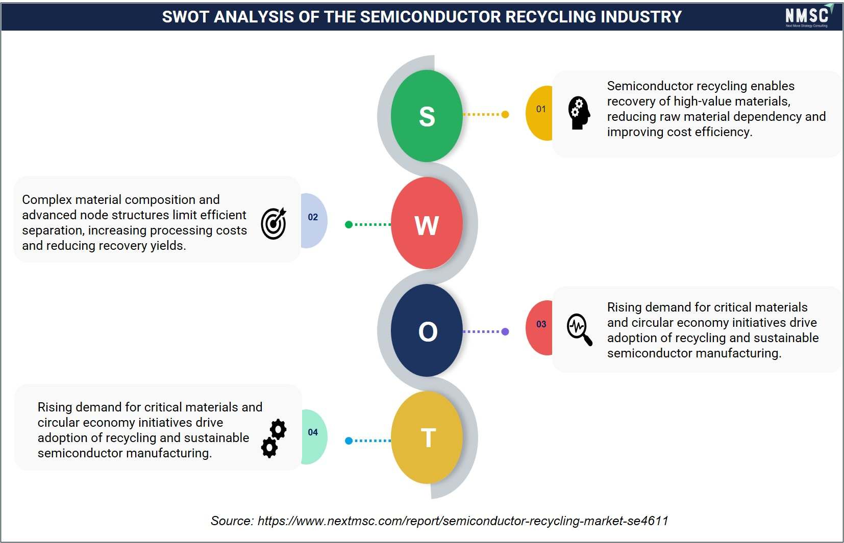
Our analysis indicates that semiconductor recycling offers strong value through recovery of critical materials, reducing dependence on primary sourcing. However, we noticed that advanced node complexity and multi-material integration limit recovery efficiency and increase processing costs. At the same time, rising demand for critical minerals and regulatory focus on circular economy create significant growth opportunities. Conversely, strict purity requirements and supply chain uncertainties remain key challenges. Nevertheless, ongoing technological advancements and policy support are expected to improve scalability and reinforce the market’s long-term strategic importance.
Competitive Landscape
Competitive Dynamics & M&A Landscape:
|
Key Takeaways |
|
The semiconductor recycling market is shaped by a mix of specialized wafer reclaim companies and large diversified materials and metals recycling firms. Key players such as Pure Wafer, Inc., RS Technologies Co., Ltd., Reldan Metals, LLC, JX Advanced Metals Corporation, DOWA Holdings Co., Ltd., TANAKA Holdings Co., Ltd., Heraeus Holding GmbH, Umicore SA/NV, Materion Corporation, Mitsubishi Materials Corporation, Sumitomo Metal Mining Co., Ltd., Veolia Environnement S.A., TES-AMM (Singapore) Pte. Ltd., Sims Lifecycle Services, Inc., Aurubis AG, Boliden AB, LS MnM Inc., Korea Zinc Co., Ltd., Asahi Pretec Corp., and PX Group S.A. leverage advanced recovery technologies, global sourcing networks, and integrated refining capabilities to maintain competitive positioning. |
|
From our assessment of competitive strategies, we found that companies increasingly focus on high-purity material recovery, closed-loop recycling partnerships with semiconductor fabs, and expansion of advanced refining capabilities. Additionally, growing emphasis on circular economy compliance, critical material recovery, and supply chain localization continues to shape service innovation and operational strategies. |
|
Recent industry developments also reflect increasing collaboration between semiconductor manufacturers and recycling service providers to secure secondary material supply. Strategic investments in recycling infrastructure, technology upgrades, and regional expansion enable companies to strengthen supply chain resilience, improve material recovery efficiency, and enhance their role within the global semiconductor ecosystem. |
Which Companies Dominate the Semiconductor Recycling Market and How Do They Compete?
Based on our analysis, we evaluated that the semiconductor recycling market is dominated by a combination of wafer reclaim specialists and global metal refining companies. Pure Wafer, RS Technologies, and Silicon Materials Inc. continue to lead wafer reclaim operations, particularly in high-volume semiconductor manufacturing environments where cost optimization and material reuse are critical. From our implementation reviews, we found that these companies were frequently selected for reclaiming test wafers, monitor wafers, and prime wafers, where maintaining semiconductor-grade quality standards is essential. At the same time, large-scale refining and materials companies such as JX Advanced Metals, Dowa Holdings, Tanaka Holdings, Heraeus, and Umicore dominated the recovery of precious and rare metals from semiconductor scrap. Competition at this level was primarily driven by recovery efficiency, refining capabilities, and global processing infrastructure, particularly in handling complex semiconductor waste streams.
Market Dominated by Semiconductor Recycling Giants and Specialists
From our observation, we found that the competitive landscape was further shaped by integrated recycling and resource recovery companies such as Materion, Mitsubishi Materials, Sumitomo Metal Mining, and Veolia. Our assessments indicated that these companies leveraged vertically integrated operations spanning collection, processing, and refining, enabling efficient and compliant handling of semiconductor waste. We also observed that TES and Sims Lifecycle Services gained traction through IT asset disposition and electronics lifecycle services, particularly in semiconductor equipment and data center recycling. In addition, companies such as Aurubis, Boliden, LS MnM, Korea Zinc, Asahi Pretec Corp., and PX Group played a critical role in extracting high-value metals such as gold, silver, palladium, and copper from semiconductor manufacturing waste. In practice, wafer reclaim specialists focused on reuse efficiency, while integrated recyclers and refiners maximized material recovery, together supporting circularity in the semiconductor value chain.
Innovation and Adaptability Drive Market Success
Innovation remains a core determinant of competitive advantage in the semiconductor recycling market, as observed through our assessments of operational facilities and pilot programs across electronics and semiconductor ecosystems. Market leaders such as Umicore, Heraeus, Mitsubishi Materials, and JX Advanced Metals advanced capabilities in hydrometallurgical processing, low-emission refining, and digital tracking systems, enabling more efficient recovery of critical materials while reducing environmental impact. From stakeholder feedback, we identified that companies investing in advanced separation technologies, AI-driven material identification, and energy-efficient processes were better positioned to scale operations and meet evolving regulatory and ESG requirements. These innovations reflect deep expertise in materials science, chemical processing, and circular economy integration, allowing suppliers to adapt to increasingly complex waste streams and sustain long-term industry relevance.
Market Players to Opt for Merger & Acquisition Strategies to Expand Their Presence
Based on our primary research, we noticed that mergers and acquisitions emerged as a key growth lever in the semiconductor recycling market as companies sought to expand technological capabilities and strengthen their global presence. Leading players increasingly targeted firms specializing in advanced recycling technologies, regional collection networks, and semiconductor-specific waste processing to enhance end-to-end service offerings. A notable example is Veolia, which, in November 2025, agreed to acquire Clean Earth from Enviri for USD 3.04 billion, significantly expanding its hazardous waste footprint in the U.S. and strengthening its position in high-growth semiconductor and advanced manufacturing sectors. Rather than focusing solely on scale, M&A strategies increasingly prioritize faster innovation cycles, improved value chain integration, and expansion into high-value electronics and semiconductor recycling. These moves help companies enhance recovery efficiency, reduce operational complexity, and secure long-term access to critical materials, driving continued consolidation across the market.
List of Key Semiconductor Recycling Companies
-
Pure Wafer, Inc.
-
RS Technologies Co., Ltd.
-
Reldan Metals, LLC
-
JX Advanced Metals Corporation
-
DOWA Holdings Co., Ltd.
-
TANAKA Holdings Co., Ltd.
-
Heraeus Holding GmbH
-
Umicore SA/NV
-
Materion Corporation
-
Mitsubishi Materials Corporation
-
Sumitomo Metal Mining Co., Ltd.
-
Veolia Environnement S.A.
-
TES-AMM (Singapore) Pte. Ltd.
-
Sims Lifecycle Services, Inc.
-
Aurubis AG
-
Boliden AB
-
LS MnM Inc.
-
Korea Zinc Co., Ltd.
-
Asahi Pretec Corp.
-
PX Group S.A.
What Are the Latest Key Industry Developments?
-
March 2026 – JX Advanced Metals completed a mass production line for high-purity CVD/ALD materials at its Ibaraki Office. This expansion is designed to ramp up shipments for advanced semiconductor node.
-
March 2026 – Mitsubishi Materials signed a Memorandum of Understanding (MoU) to acquire shares in ReElement Technologies Corporation. This partnership focuses on high-purity rare earth and critical mineral recovery, strengthening the Japan-U.S. supply chain for semiconductor materials.
-
March 2026 – Dowa Ecosystem and Kuraray launched a joint study into a new resource circulation business. This partnership focuses specifically on the reactivation of activated carbon, a critical component in the filtration and waste treatment processes of semiconductor manufacturing facilities.
Expert Insights
 "While it is important to manufacture semiconductors using new advanced technologies, it is also meaningful to protect the legacy semiconductor ecosystem where the majority of demand occurs."
Kim Jung-woong, CEO of Surplus Global
Statement made while discussing the importance of preserving and extending the lifecycle of legacy semiconductor manufacturing infrastructure through reuse, refurbishment, and ecosystem sustainability.
Market Interpretation
The statement highlights the growing strategic importance of semiconductor recycling and equipment refurbishment as manufacturers seek to extend the operational life of legacy fabrication assets. A significant portion of global semiconductor demand continues to rely on mature-node production used in automotive, industrial electronics, power devices, and consumer applications, creating sustained demand for reused tools, recovered components, and refurbished process equipment. As a result, semiconductor manufacturers and foundries are increasingly investing in recycling, asset recovery, and equipment remanufacturing to reduce capital expenditure, improve supply chain resilience, and support sustainable manufacturing practices. This trend is accelerating the adoption of semiconductor recycling solutions and creating long-term growth opportunities across the global semiconductor recycling market.
What Are the Key Factors Influencing Investment Analysis & Opportunities in the Semiconductor Recycling Market?
Investment analysis in the semiconductor recycling market is increasingly shaped by a shift toward technology-driven and integrated recycling platforms, rather than conventional material recovery operations. Based on our evaluation of recent funding activity, strategic partnerships, and capacity expansion initiatives, we identified that investors favour companies with advanced recovery technologies, high-purity processing capabilities, and scalable recycling infrastructure. Firms demonstrating efficient material recovery, process automation, and strong integration with semiconductor manufacturing workflows consistently attract higher strategic interest.
We also identified investment concentration around precision material recovery, wafer reclaim optimization, and digital traceability systems that enhance transparency and resource efficiency. Strategic investments are gaining prominence, as semiconductor manufacturers, materials companies, and recycling firms seek tighter control over material supply chains and circular production models. For investors, the most compelling opportunities lie in companies combining technological differentiation with operational scalability, consistent recovery yields, and the ability to support closed-loop recycling ecosystems within the semiconductor industry.
Key Benefits for Stakeholders:
Next Move Strategy Consulting (NMSC) presents a comprehensive analysis of the market, covering historical developments from 2020 to 2025 and providing forward-looking forecasts through 2035. The study evaluates the market at global, regional, and country levels, delivering quantitative outlooks alongside qualitative insights into material recovery trends, process advancements, circularity adoption, and investment patterns across all major semiconductor recycling market segments.
From our observation, the semiconductor recycling industry delivers measurable value across the ecosystem. Investors benefit from growing demand for high-value material recovery and scalable recycling models supported by circular economy initiatives. Semiconductor manufacturers gain cost optimization and supply stability through reuse of wafers and critical materials. Recycling service providers, equipment suppliers, and technology developers benefit from long-term processing contracts, technology upgrades, and expanding recovery capabilities. By aligning advanced recycling processes with material efficiency and supply chain resilience, the market creates sustained value while supporting long-term sustainability and resource security.
|
Parameters |
Details |
|
Customization Scope |
Free customization (equivalent to up to 80 analyst-working hours) after purchase. Addition or alteration to country, regional & segment scope. |
|
Pricing and Purchase Options |
Avail customized purchase options to meet your exact research needs. |
|
Approach |
In-depth primary and secondary research; proprietary databases; rigorous quality control and validation measures. |
|
Analytical Tools |
Porter's Five Forces, SWOT, value chain, and Harvey ball analysis to assess competitive intensity, stakeholder roles, and relative impact of key factors. |
Semiconductor Recycling Market Key Segments
By Feedstock Source
-
Wafer Reclaim
-
Prime Wafers
-
Test Wafers
-
Dummy Wafers
-
-
Fab Scrap
-
Wafer Rejects
-
Edge Trim
-
Kerf Loss
-
Process Residues
-
CMP Slurry
-
Spent Chemicals
-
Sludge
-
-
Assembly Scrap
-
Leadframes
-
Substrates
-
Package Scrap
-
Test Scrap
-
-
Facility Scrap
-
Quartzware
-
Ceramics
-
Filters
-
Metal Parts
-
Abatement Media
-
-
R&D Scrap
-
Pilot Wafers
-
Prototype Scrap
-
By Recovered Output
-
Reclaimed Wafers
-
Silicon
-
SiC
-
Other Compound
-
-
Metals
-
Precious Metals
-
Gold
-
Silver
-
Palladium
-
Platinum
-
-
Base Metals
-
Copper
-
Aluminum
-
Tin
-
Nickel
-
-
Specialty Metals
-
Tantalum
-
Cobalt
-
Indium
-
Gallium
-
-
-
Chemicals
-
Acids
-
Solvents
-
Bases
-
Photoresist
-
-
Parts
-
Photomasks
-
Reticles
-
Quartzware
-
Carriers
-
Boats
-
-
Other Outputs
By Processing Route
-
Mechanical
-
Chemical
-
Thermal
-
Electrochemical
-
Membrane
-
Direct Reclaim
By Commercial Model
-
Tolling
-
Fee For Service
-
Treatment Contract
-
-
Merchant
-
Scrap Purchase
-
Resale of Recovered Material
-
-
Hybrid
Geographical Breakdown
-
North America: U.S., Canada, and Mexico.
-
Europe: UK, Germany, France, Italy, Spain, Sweden, Denmark, Finland, the Netherlands, and the Rest of Europe.
-
Asia Pacific: China, India, Japan, South Korea, Taiwan, Indonesia, Vietnam, Australia, Philippines, Malaysia and the rest of APAC.
-
Middle East & Africa (MEA): Saudi Arabia, UAE, Egypt, Israel, Turkey, Nigeria, South Africa, and the rest of MEA.
-
Latin America: Brazil, Argentina, Chile, Colombia, and the rest of LATAM.
Conclusion & Recommendations
This report provides stakeholders, service providers, investors, and consultants with actionable insights to capitalise on the structural transformation underway in the market. By combining rigorous data-driven analysis with structured evaluation of semiconductor value chains, NMSC’s Semiconductor Recycling Market Report serves as a critical decision-support resource for navigating an increasingly resource-constrained and sustainability-driven industry landscape. The market is positioned for sustained expansion, supported by rising material costs, growing semiconductor production volumes, and increasing regulatory emphasis on circular economy practices. Key strategic insights highlight the shift toward advanced material recovery, wafer reclaim optimization, and digital traceability frameworks, as these capabilities strengthen supply security and improve cost efficiency. Market participants that prioritize high-purity recovery technologies, process automation, and integrated recycling solutions consistently strengthen operational resilience and long-term value creation across semiconductor ecosystems.
For executives and investors, capturing value requires focusing on high-impact areas such as wide-bandgap material recovery, chiplet-level reuse, and closed-loop recycling models, while continuing investments in advanced processing technologies, digital tracking systems, and strategic partnerships with semiconductor manufacturers. Expanding presence in key semiconductor hubs, particularly Asia-Pacific, the United States, and Europe, unlocks access to high-volume scrap streams and established manufacturing ecosystems. Process scalability, material purity, and supply chain integration further strengthen competitive positioning and accelerate adoption, enabling recycling to evolve into a strategic pillar of semiconductor manufacturing and long-term resource sustainability.


About the Author
 Saista Faiyaz
— Saista Faiyaz is Research Associate at Next Move Strategy Consulting, where she has covered consumer markets and healthcare technologies for 3 years. Her work includes primary interview review, secondary-source validation, market sizing, and structured analysis of company and industry data. She supports research by comparing evidence across sources, organizing findings into market narratives, and documenting assumptions used in analysis. Her scope includes cross-market benchmarking, and reports.
Saista Faiyaz
— Saista Faiyaz is Research Associate at Next Move Strategy Consulting, where she has covered consumer markets and healthcare technologies for 3 years. Her work includes primary interview review, secondary-source validation, market sizing, and structured analysis of company and industry data. She supports research by comparing evidence across sources, organizing findings into market narratives, and documenting assumptions used in analysis. Her scope includes cross-market benchmarking, and reports.
About the Reviewer
 Supradip Baul
— Supradip Baul is an accomplished business consultant and strategist with over a decade of rich experience in market intelligence, strategy, technology, and business transformation. His work has included rigorous qualitative and quantitative analysis across multiple industries, helping clients shape investment decisions and long-term roadmaps. Earlier in his career, he was associated with Gartner, where he contributed to industry-leading reports and market share analyses. He has worked with leading global companies and holds an MBA with a dual specialization in Marketing and Finance.
Supradip Baul
— Supradip Baul is an accomplished business consultant and strategist with over a decade of rich experience in market intelligence, strategy, technology, and business transformation. His work has included rigorous qualitative and quantitative analysis across multiple industries, helping clients shape investment decisions and long-term roadmaps. Earlier in his career, he was associated with Gartner, where he contributed to industry-leading reports and market share analyses. He has worked with leading global companies and holds an MBA with a dual specialization in Marketing and Finance.
At Next Move Strategy Consulting, we understand that insightful market research is the cornerstone of successful business decisions. That's why we employ a robust and multifaceted approach, combining various methodologies to deliver the most accurate and actionable data for our clients.

Research Landscape
We navigate the world of research with two primary approaches:
Qualitative Approach
Our qualitative research methodologies involve immersive techniques such as in-depth interviews, focus groups, and observational studies. By engaging directly with individuals and stakeholders, we uncover valuable insights that quantitative data alone may overlook.

Quantitative Research
In tandem with qualitative methodologies, NMSC leverages the power of Quantitative Research to provide a robust foundation of numerical insights. Through systematic data collection and analysis, we quantify patterns, preferences, and market trends, offering a comprehensive view of the business landscape.
Our quantitative research approach employs diverse tools, including surveys, experiments, and statistical modelling. These methodologies enable us to gather data from a large and representative sample, ensuring the statistical significance of our findings. By employing structured questionnaires and standardized data collection methods, we guarantee the reliability and validity of the information we present to our clients.
Quantitative research is particularly effective in measuring the prevalence of trends, assessing market size, and gauging the impact of various factors on consumer behavior. The numerical precision attained through this approach equips our clients with actionable insights, facilitating data-driven decision-making and strategy formulation.


Our Specialized Toolbox for Industry-Specific Market Research
We deploy a specialized arsenal of techniques tailored to meet your unique requirements. Here's a glimpse into our comprehensive toolbox:

Information Procurement
The stage entails acquiring market data or relevant information through various sources and methodologies.


Market Research Approach
We utilize both top-down and bottom-up approaches in market research analysis to achieve a comprehensive understanding of the market dynamics, leveraging the broad perspective of industry trends and macroeconomic factors alongside detailed insights from specific segments and individual companies.

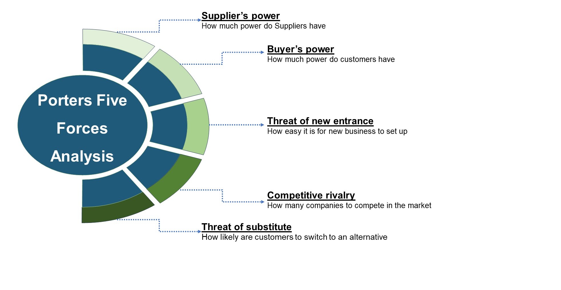
Porters Five Forces Analysis
We conduct Porter's Five Forces analysis to evaluate the competitive landscape of an industry, providing us with insights into factors that affect profitability and strategic positioning.
SWOT Analysis

Forecasting
We utilize a forecasting model to predict future consumption by considering parameters like population, economics, regulations, market competition, drivers, constraints, technology, and pricing. We also employ statistical techniques such as multilinear regression, exponential smoothing, moving average, ARIMA, and Monte Carlo simulations for accurate predictions. In econometric forecasting, we analyzed short-term and long-term event impacts, attributing values based on regulatory frameworks, economic factors, and market events.





 Speak to Our Analyst