Advanced Packaging Emerges as AI's Critical Bottleneck
TSMC and Intel Race to Build U.S. Advanced Packaging Capacity as Nvidia Locks Up Global Supply, Reshaping the Global Semiconductor Packaging Market
An underappreciated step in the chipmaking process has moved to the center of the global technology industry's most consequential strategic contest. On April 8, 2026, CNBC reported that Nvidia has reserved the majority of TSMC's most advanced chip packaging capacity, while TSMC prepares to break ground on its first U.S. advanced packaging facilities in Arizona, and Elon Musk's Terafab project taps Intel for custom chip packaging for SpaceX, xAI, and Tesla. The report — based on rare access to both TSMC and Intel packaging operations — identified advanced packaging as the next critical bottleneck for artificial intelligence infrastructure, a development with far-reaching implications for the global Semiconductor Packaging Market.
For More Information: Download FREE Sample on Semiconductor Packaging Market Report
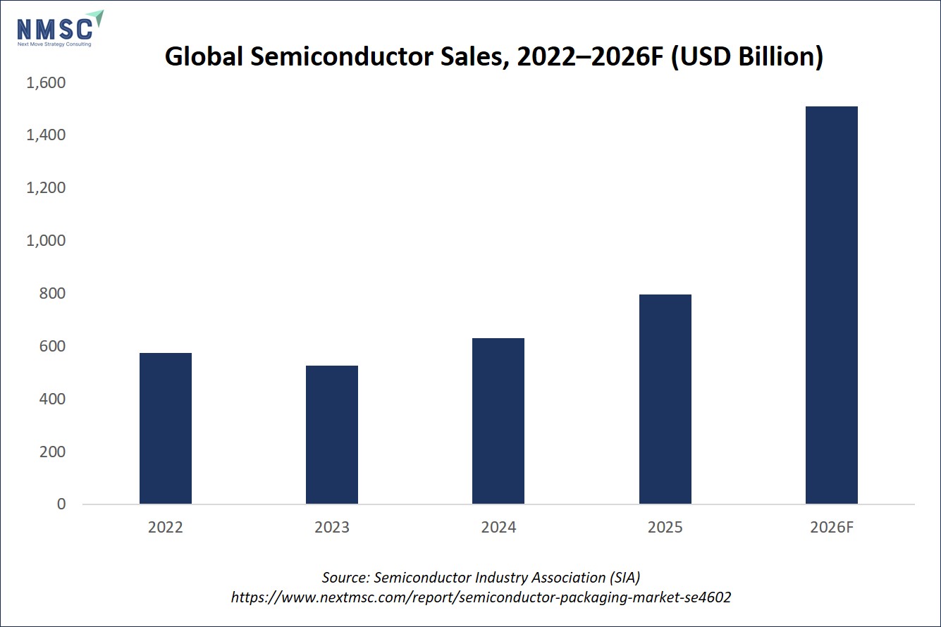
The timing of this supply-side scramble is significant. According to the Semiconductor Industry Association (SIA), global semiconductor sales reached $795.6 billion in 2025, surpassing initial forecasts, and the World Semiconductor Trade Statistics (WSTS) organization projects worldwide semiconductor sales will reach $1.51 trillion in 2026 — a 90% year-over-year expansion driven overwhelmingly by memory and logic products serving AI infrastructure. Within this broader industry surge, advanced packaging has emerged as the critical enabling layer that determines whether chip performance gains can be realized at scale.
Market Valuation and Growth Trajectory
According to Next Move Strategy Consulting (NMSC), the global semiconductor packaging market was valued at USD 68.44 billion in 2025 and is projected to reach USD 74.83 billion by the end of 2026. The market is forecast to expand to USD 167.14 billion by 2035, representing a compound annual growth rate (CAGR) of 9.34% over the 2026–2035 forecast period. This trajectory reflects a structural transformation in which packaging has evolved from a backend manufacturing process into a primary performance enabler for next-generation semiconductor architectures.
NMSC's analysis, drawn from engagement with semiconductor ecosystem participants, identifies rising demand for AI processors, high-performance computing (HPC), and advanced automotive electronics as the primary structural growth catalysts. Increasing chip complexity and the shift toward chiplet-based architectures and heterogeneous integration are redefining packaging from a cost center into a critical competitive differentiator.
The Advanced Packaging Bottleneck
TSMC's most advanced packaging method currently in commercial use — Chip on Wafer on Substrate, or CoWoS — is growing at an 80% compound annual growth rate, according to TSMC North America packaging solutions head Paul Rousseau, as reported by CNBC in April 2026. Nvidia has reserved the majority of this capacity, and demand is so acute that TSMC has reportedly outsourced portions of the process to third-party OSAT providers including ASE and Amkor Technology. ASE, the world's largest outsourced semiconductor assembly and test company, projects its advanced packaging sales to double to approximately $32 billion in 2026, according to Reuters.
The capacity constraint is structural. TSMC currently sends 100% of chips — including those fabricated at its advanced plant in Phoenix, Arizona — to Taiwan for packaging. The company is now building two new packaging facilities in Arizona and ramping two additional sites in Taiwan to address the shortfall. Intel, meanwhile, already conducts portions of its most advanced packaging near its 18A fabrication plant in Arizona, with packaging customers including Amazon, Cisco, and, as of April 2026, SpaceX, xAI, and Tesla through Musk's Terafab project.
"It can emerge as a bottleneck very quickly if people are not making the CapEx investments proactively to account for the surge in fab output that's going to be coming in the next couple of years," said John VerWey of Georgetown University's Center for Security and Emerging Technology, as quoted by CNBC.
AI Infrastructure as the Primary Demand Catalyst
The SIA's 2026 State of the U.S. Semiconductor Industry report, published July 27, 2026, underscores the scale of AI-driven semiconductor demand. A single AI server rack contains more than 4,500 packaged semiconductors, with chips representing more than 95% of an AI server rack's value and more than half of total AI data center capital expenditures. Government and industry are expected to invest more than $4 trillion in AI data center infrastructure globally through 2028, with up to $2.8 trillion dedicated to semiconductors, according to SIA and Deloitte research.
This demand profile directly elevates the strategic importance of advanced packaging. NMSC's analysis indicates that AI workloads require ultra-high bandwidth, low latency, and efficient power delivery — performance characteristics that conventional packaging architectures cannot support. High-bandwidth memory (HBM), including HBM3e and emerging HBM4, requires 3D stacking and through-silicon via (TSV) technologies that enable vertical memory integration, reducing signal delay and improving data throughput in AI accelerators and data center processors.
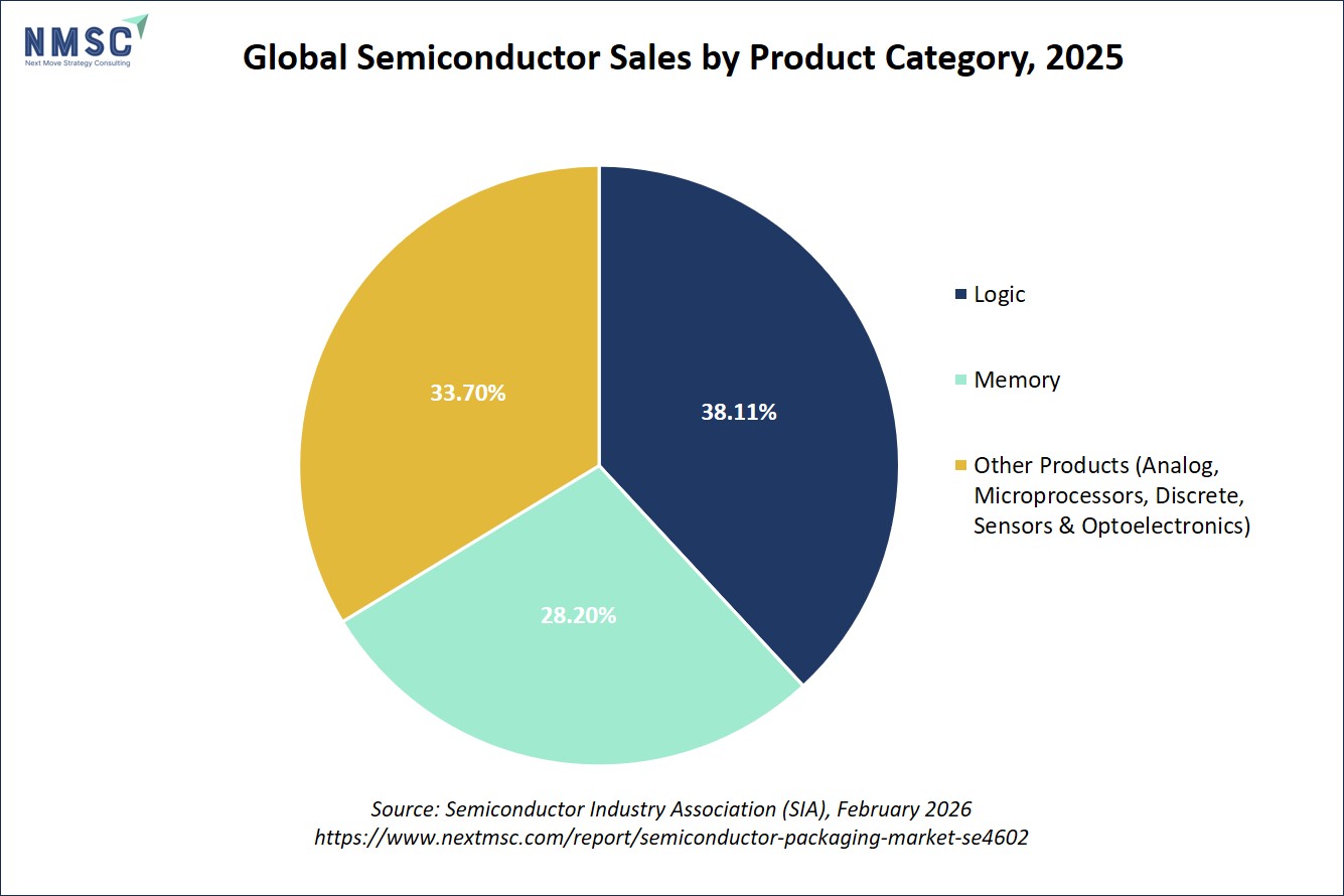
In 2025, sales of logic products increased by 39.9%, totaling $301.9 billion — the largest product category by sales — while memory products increased by 34.8% to $223.1 billion, according to SIA. These two categories alone accounted for approximately 66.3% of global semiconductor sales in 2025, reflecting the concentrated demand from AI and data center applications.
Technology Architecture: From 2D to 3D Integration
The industry is undergoing a fundamental architectural transition. NMSC's market analysis identifies the shift from monolithic chip designs to modular chiplet-based architectures as a foundational trend reshaping packaging requirements. The emergence of the UCIe (Universal Chiplet Interconnect Express) standard is enabling interoperability between chiplets from multiple vendors, reducing design complexity while accelerating time to market for advanced processors.
TSMC's CoWoS represents the current commercial frontier of 2.5D packaging, using a high-density wiring interposer to mount high-bandwidth memory directly adjacent to compute chips. Nvidia's Blackwell GPUs are the first product manufactured using TSMC's latest CoWoS-L generation. Intel's competing technology — embedded multi-die interconnect bridge (EMIB) — achieves similar results using silicon bridges embedded within the package, offering a cost advantage through selective placement.
Both companies are also advancing 3D packaging. TSMC's System on Integrated Chips (SoIC) and Intel's Foveros Direct stack dies vertically, enabling chips to function as a unified unit — delivering a new level of performance gain, as TSMC's Rousseau described to CNBC. Memory companies including Samsung, SK Hynix, and Micron are deploying 3D packaging to stack dies into high-bandwidth memory modules, with hybrid bonding — replacing solder bumps with copper pad-to-pad connections — emerging as the next performance frontier.
Co-packaged optics (CPO) is also gaining traction as a solution to bandwidth and thermal limitations in modern data centers. By integrating optical engines directly into semiconductor packages using silicon photonics, CPO architectures enable higher bandwidth density and improved energy efficiency for AI-driven workloads. NMSC's analysis identifies CPO as a next-generation packaging approach for high-performance data infrastructure, particularly in 800G and 1.6T network environments.
Glass substrates represent an additional frontier. NMSC's assessment identifies Intel Corporation and Samsung Electronics as leading the transition toward glass substrates, which offer superior dimensional stability, improved thermal resistance, and higher interconnect density compared to traditional organic materials — positioning them as a key enabler for next-generation processors in generative AI training environments.
Policy Landscape and Capital Investment
The geopolitical dimension of advanced packaging has prompted significant policy intervention across major economies. The U.S. CHIPS and Science Act, enacted in 2022, appropriated approximately USD 53 billion over five years for semiconductor manufacturing incentives, R&D, and workforce development, including a 25% investment tax credit for qualifying facilities. The CHIPS National Advanced Packaging Manufacturing Program (NAPMP) finalized USD 1.4 billion in award funding in 2025 to strengthen advanced packaging capabilities in the United States, according to the U.S. Department of Commerce.
In Europe, the European Chips Act — which came into force in September 2023 — aims to double the EU's global semiconductor market share to 20% by 2030. According to the European Commission in 2026, the Act has mobilized more than USD 91 billion in semiconductor-related investments across design, pilot lines, packaging, and manufacturing activities. Japan's "Strategy for Semiconductor and the Digital Industry" targets more than JPY 15 trillion in domestically produced semiconductor sales by 2030, supported by tax breaks, subsidies, and public financial support for ventures including Rapidus Corp.
The OECD, in its September 2025 report "Economic Security in a Changing World," identified semiconductor production as the most geographically concentrated industry in its database, with approximately 75% of value-added generated by five economies — four of which are in Asia. The report warned that disruption in any leading economy within the semiconductor value chain could precipitate widespread shortages affecting diverse downstream industries worldwide, reinforcing the policy rationale for geographic diversification of packaging capacity.
Since 2020, semiconductor companies have announced more than $770 billion in private-sector investments across 160 projects in 30 U.S. states, strengthening domestic manufacturing, equipment production, materials, packaging, and research capabilities, according to SIA.
Global Semiconductor Sales by Region — Annual Growth Rates, 2025
|
Region |
2025 YoY Sales Growth |
Primary Growth Driver |
|
Asia Pacific / All Others |
+45.0% |
AI server hardware, consumer electronics manufacturing |
|
Americas |
+30.5% |
AI infrastructure, cloud computing, data center expansion |
|
China |
+17.3% |
Consumer electronics, telecom infrastructure, AI hardware |
|
Europe |
+6.3% |
Automotive electronics, industrial automation |
|
Japan |
–4.7% |
Legacy semiconductor demand contraction |
|
Global Total |
+25.6% |
AI, memory, and logic product demand |
Regional Market Dynamics
Asia-Pacific remains the dominant manufacturing hub for semiconductor packaging, anchored by TSMC in Taiwan, Samsung Electronics and SK Hynix in South Korea, and a network of OSAT providers including ASE, Amkor Technology, and Tongfu Microelectronics. NMSC's regional analysis identifies Taiwan as a critical center for advanced packaging technologies including CoWoS and integrated fan-out packaging, while South Korea leads in high-bandwidth memory packaging for AI applications.
North America is accelerating its domestic packaging capabilities through a combination of private investment and policy incentives. TSMC's Arizona packaging facilities, Intel's existing U.S. packaging operations, and the CHIPS Act's NAPMP program collectively represent a strategic effort to reduce dependence on Asian packaging capacity. NMSC's analysis notes that North America's focus on cutting-edge packaging innovation and chiplet ecosystems positions the region as a center for advanced packaging development, even as volume manufacturing remains concentrated in Asia-Pacific.
Europe's semiconductor packaging market is anchored in automotive electronics, industrial automation, and power semiconductor applications. The region's stringent regulatory environment and emphasis on thermally stable, energy-efficient packaging solutions — particularly for electric vehicles and industrial equipment — create a differentiated demand profile. Germany's engineering-intensive automotive sector and France's aerospace and defense applications represent the primary demand drivers.
Emerging regions including India and Southeast Asia are gradually strengthening assembly and packaging capabilities, supported by policy initiatives and ecosystem investments. NMSC's analysis identifies these regions as increasingly important participants in the global semiconductor packaging supply chain, particularly for cost-efficient, high-volume assembly and test operations.
Key Industry Developments
Several corporate developments in the past twelve months have reshaped the competitive landscape. In March 2026, Intel confirmed the readiness of its Intel 18A process technology featuring RibbonFET and PowerVia architectures, supporting next-generation AI and high-performance computing applications. In February 2026, Renesas Electronics Corporation signed a definitive agreement to transfer its timing business to SiTime Corporation in a transaction valued at approximately USD 1.5 billion, alongside an MoU to develop integrated solutions combining SiTime's MEMS resonators with Renesas MCUs and SoCs through bare-die co-packaging. In October 2025, NXP Semiconductors completed the acquisitions of Aviva Links for USD 243 million and Kinara for USD 307 million, strengthening its automotive connectivity and AI-powered edge computing capabilities.
Key Semiconductor Packaging Industry Developments, October 2025 – April 2026
|
Date |
Company / Entity |
Development |
Strategic Significance |
|
October 2025 |
NXP Semiconductors |
Acquired Aviva Links (USD 243M) and Kinara (USD 307M) |
Strengthens automotive AI edge computing and connectivity packaging |
|
February 2026 |
ASE Technology |
Advanced packaging sales projected to double to ~USD 32B |
Signals OSAT capacity expansion driven by AI packaging demand |
|
February 2026 |
Renesas / SiTime |
USD 1.5B timing business transfer + bare-die co-packaging MoU |
Advances semiconductor integration and device miniaturization |
|
March 2026 |
Intel Corporation |
Intel 18A process readiness confirmed (RibbonFET + PowerVia) |
Enables next-generation AI and HPC advanced packaging |
|
April 2026 |
TSMC |
Breaking ground on two advanced packaging facilities in Arizona |
First U.S.-based advanced packaging capacity for TSMC |
|
April 2026 |
Nvidia / TSMC |
Nvidia reserves majority of TSMC CoWoS capacity; CoWoS growing at 80% CAGR |
Confirms advanced packaging as AI supply chain's critical constraint |
Automotive Electrification as a Secondary Growth Driver
Beyond AI, automotive electrification represents a significant structural demand driver for advanced semiconductor packaging. The transition toward electric vehicles and high-voltage (800V) architectures is increasing demand for silicon carbide (SiC) and gallium nitride (GaN) power semiconductors, which operate under extreme thermal and electrical conditions requiring robust packaging solutions. Infineon Technologies achieved a major milestone in 200mm SiC production in 2025, enabling scalable, high-volume manufacturing of power semiconductors for electric vehicles — a development that directly increases demand for thermally efficient packaging technologies.
NMSC's analysis identifies automotive electrification as contributing a +1.2% impact on the semiconductor packaging market's CAGR forecast, with geographic relevance concentrated in Europe (Germany), Asia-Pacific (Japan, China), and North America. The integration of electronic control units, ADAS systems, and EV powertrain electronics is driving demand for compact, high-efficiency packaging formats capable of sustained performance under demanding thermal and electrical conditions.
Competitive Landscape
The semiconductor packaging market is dominated by large integrated device manufacturers (IDMs) and leading foundries alongside specialized OSAT providers. Intel Corporation, Samsung Electronics, and TSMC consistently lead in advanced packaging deployments where performance optimization, chiplet integration, and high-bandwidth requirements are critical. Amkor Technology strengthens its position as a leading OSAT provider by offering scalable, cost-efficient packaging solutions across consumer electronics, automotive, and industrial segments.
Competition is further shaped by IDM and application-specific players including Texas Instruments, Infineon Technologies, NXP Semiconductors, STMicroelectronics, and Renesas Electronics, which gain traction through in-house and hybrid packaging models tailored to power electronics, automotive, and industrial applications. NMSC's competitive assessment identifies innovation in heterogeneous integration, 2.5D/3D packaging, and system-in-package (SiP) technologies as the primary determinants of competitive advantage, with companies investing in advanced substrates and thermal management solutions better positioned to serve AI, automotive electrification, and HPC demand.
U.S.-headquartered companies generated $425 billion in semiconductor sales in 2025, accounting for 53.4% of worldwide market share — the highest U.S. share since 1984 — and invested a record $76.8 billion in research and development, reinforcing the industry's position as one of the world's most research-intensive sectors.
Investment Implications
The convergence of AI infrastructure demand, automotive electrification, and geopolitical supply chain restructuring creates a multi-vector investment thesis for the semiconductor packaging market. NMSC's assessment identifies 2.5D/3D packaging, heterogeneous integration, chiplet architectures, and system-in-package (SiP) technologies as the primary areas of capital allocation by semiconductor manufacturers and OSAT providers.
The capital intensity of advanced packaging infrastructure remains a significant constraint. Building a manufacturing plant for leading-edge semiconductors requires an upfront investment of USD 10–20 billion, according to OECD analysis, with long lead times and access to a highly specialized talent pool. This cost burden creates strong entry barriers for smaller market participants and extends payback periods, limiting the pace of capacity expansion relative to demand growth — a dynamic that reinforces the competitive moat of established IDMs and OSAT leaders.
Bottom Line
The global semiconductor packaging market stands at a structural inflection point, driven by the convergence of AI infrastructure demand, automotive electrification, and geopolitical supply chain restructuring. The April 2026 revelation that Nvidia has reserved the majority of TSMC's most advanced packaging capacity — while TSMC and Intel race to establish U.S.-based packaging facilities — underscores that advanced packaging has transitioned from a backend manufacturing step to a strategic chokepoint in the global technology supply chain. With the market projected to expand from USD 74.83 billion in 2026 to USD 167.14 billion by 2035 at a CAGR of 9.34%, according to NMSC, the investment opportunity is substantial. However, risks are material: geographic concentration of packaging capacity in Asia-Pacific, high capital expenditure requirements exceeding USD 10–20 billion per facility, and intensifying geopolitical tensions over semiconductor supply chains create execution uncertainty. For investors and industry participants, the strategic imperative is clear — companies that secure advanced packaging capacity, invest in heterogeneous integration capabilities, and build resilient supply chain partnerships across North America, Europe, and Asia-Pacific will be best positioned to capture value in the next decade of semiconductor industry growth.
About Next Move Strategy Consulting
Next Move Strategy Consulting is a premier market research and management consulting firm that has been committed to provide strategically analysed well documented latest research reports to its clients. The research industry is flooded with many firms to choose from, what makes NMSC different from the rest is its top-quality research and the obsession of turning data into knowledge by dissecting every bit of it and providing fact-based research recommendation that is supported by information collected from over 500 million websites, paid databases, industry journals and one on one consultations with industry experts across a diverse range of industry sectors. The high-quality customized research reports with actionable insights and excellent end-to-end customer service help our clients to take critical business decisions that enables them to move beyond time and have competitive edge in the industry.
We have been servicing over 1000 customers globally that includes 90% of the Fortune 500 companies over a decade. Our analysts are constantly tracking various high growth markets and identifying hidden opportunities in each sector or the industry. We provide one of the industry's best quality syndicate as well as custom research reports across 10 different industry verticals. We are committed to deliver high quality research solutions in accordance to your business needs. Our industry standard delivery solutions that ranges from the pre consultation to after-sales services, provide an excellent client experience and ensure right strategic decision making for businesses.
For more information, please contact:
Next Move Strategy Consulting
5th Floor 867 Boylston St, STE 500,
Boston, MA 02116, U.S.
E-Mail: [email protected]
Direct: +1-217-650-7991
Website: www.nextmsc.com
About the Author
 Sanyukta Deb
— Sanyukta Deb is Digital Marketing Team Lead at Next Move Strategy Consulting, where she has led content strategy and technical SEO for the firm's B2B market research publications for over 2 years. Her editorial process translates NextMSC's primary and secondary research — spanning technology, industrial, and consumer sectors — into commercial narratives, backed by search-intent, keyword, and competitive analysis. She brings 5 years of overall experience in digital marketing and content strategy.
Sanyukta Deb
— Sanyukta Deb is Digital Marketing Team Lead at Next Move Strategy Consulting, where she has led content strategy and technical SEO for the firm's B2B market research publications for over 2 years. Her editorial process translates NextMSC's primary and secondary research — spanning technology, industrial, and consumer sectors — into commercial narratives, backed by search-intent, keyword, and competitive analysis. She brings 5 years of overall experience in digital marketing and content strategy.
About the Reviewer
 Debashree Dey
— Debashree Dey is Assistant Manager at Next Move Strategy Consulting, where she supports cross-vertical market content and communications across diverse industries for 6 years. Her professional background includes senior content writing, communications, and published manuscript authorship, with experience developing audience-focused business narratives and maintaining clear, consistent messaging. Her role supports research-led content development and editorial quality across NextMSC publications.
Debashree Dey
— Debashree Dey is Assistant Manager at Next Move Strategy Consulting, where she supports cross-vertical market content and communications across diverse industries for 6 years. Her professional background includes senior content writing, communications, and published manuscript authorship, with experience developing audience-focused business narratives and maintaining clear, consistent messaging. Her role supports research-led content development and editorial quality across NextMSC publications.














Add Comment