Chiplet Market: Heat Emerges as AI's Core Bottleneck
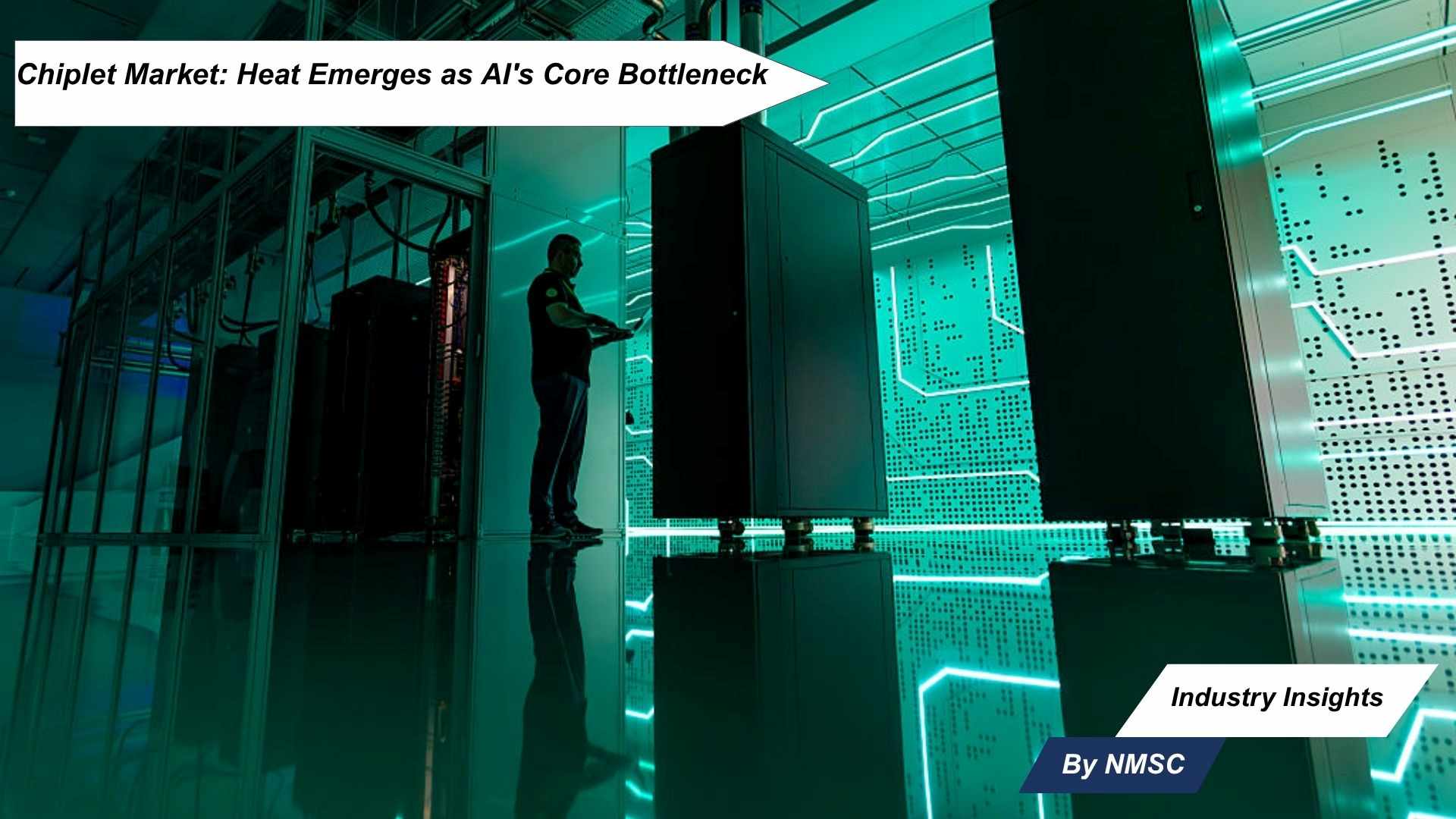
Chip Packaging Experts Warn Thermal Limits Could Constrain AI as 3D Chiplet Stacking Scales
SEOUL, South Korea August 21, 2026 Leading semiconductor packaging researchers have issued a formal warning that thermal management is rapidly becoming the most critical constraint on AI infrastructure expansion, as the widespread adoption of three-dimensional (3D) stacking in both system semiconductors and memory chiplets intensifies heat generation across advanced packaging architectures. The development carries direct implications for the Chiplet Market, which was valued at USD 10.97 billion in 2024 and is projected to reach USD 243.47 billion by 2030, expanding at a CAGR of 68.8% from 2025 to 2030, according to Next Move Strategy Consulting.
KAIST Professor Kim Joung-ho, speaking on the thermal challenges confronting next-generation AI chip architectures, cautioned that escalating heat demands could constrain AI expansion unless the industry adopts fundamentally new design and cooling methodologies. He identified AI-based design automation and digital twin technologies as the most viable near-term tools for reducing heat and power consumption across AI infrastructure.
Professor Kim also highlighted the emergence of next-generation memory architectures beyond High Bandwidth Memory (HBM), including HBF based on stacked NAND flash and HBS based on stacked SRAM as technologies expected to define the AI memory landscape. As these architectures grow in complexity, he stressed that thermal management will require AI-driven design automation capable of autonomously handling advanced packaging designs and identifying optimal heat dissipation solutions based on physical laws.
The thermal challenge is already reshaping product development at the foundry level. Samsung's zHBM technology, which stacks memory vertically above AI accelerators using wafer-bonding, is expected to deliver more than 10 times the memory density of HBM5, three times the energy efficiency, and more than 50% lower thermal resistance underscoring the urgency of thermal innovation within chiplet-based architectures.
Key Highlights:
-
Thermal design power (TDP) for individual AI chips from NVIDIA, AMD, and Google has surpassed 1 kilowatt, while rack-scale AI systems now consume hundreds of kilowatts, according to TrendForce data.
-
Liquid cooling penetration among AI chips is projected to rise from approximately 33% in 2025 to 53% in 2026, approaching 60% by 2027, reflecting the urgency of thermal management at scale.
-
Co-packaged optics (CPO) and system-technology co-optimization (STCO) have been identified by Seoul National University of Science and Technology Professor Kim Sung-dong as the industry's primary strategic responses to the thermal bottleneck in advanced semiconductor packaging.
-
Physics-informed neural networks (PINNs) and deep reinforcement learning are rapidly emerging as autonomous design tools for optimizing substrate warpage and power delivery networks (PDNs) in chiplet-based systems.
Analyst Insight:
According to analysts at Next Move Strategy Consulting, the thermal bottleneck identified by leading packaging researchers represents a structural inflection point for the global chiplet market. As 3D-stacked architectures become the dominant design paradigm for AI accelerators and memory, the ability to manage heat dissipation at the chiplet integration level will increasingly determine competitive differentiation among semiconductor manufacturers. NMSC analysts note that the convergence of AI-driven design automation, co-packaged optics, and advanced liquid cooling is likely to accelerate capital investment in next-generation packaging infrastructure, reinforcing the market's projected trajectory toward USD 243.47 billion by 2030.
Industry Outlook:
The warnings issued by leading semiconductor packaging researchers signal that thermal management is transitioning from a secondary engineering consideration to a primary strategic priority within the chiplet ecosystem. As AI workloads continue to scale and 3D chiplet stacking becomes more pervasive, the industry is expected to accelerate investment in AI-driven design tools, advanced cooling architectures, and novel interconnect technologies such as CPO and STCO. Vendors and foundries that successfully integrate thermal optimization into their chiplet design and packaging workflows are positioned to capture a disproportionate share of the market's growth as demand for high-performance, energy-efficient AI infrastructure intensifies globally.
Source: TrendForce
For More Information: Download FREE Sample on Chiplet Market Market Report
Prepared By: Sanyukta Deb
About the Author
 Sanyukta Deb
— Sanyukta Deb is Digital Marketing Team Lead at Next Move Strategy Consulting, where she has led content strategy and technical SEO for the firm's B2B market research publications for over 2 years. Her editorial process translates NextMSC's primary and secondary research — spanning technology, industrial, and consumer sectors — into commercial narratives, backed by search-intent, keyword, and competitive analysis. She brings 5 years of overall experience in digital marketing and content strategy.
Sanyukta Deb
— Sanyukta Deb is Digital Marketing Team Lead at Next Move Strategy Consulting, where she has led content strategy and technical SEO for the firm's B2B market research publications for over 2 years. Her editorial process translates NextMSC's primary and secondary research — spanning technology, industrial, and consumer sectors — into commercial narratives, backed by search-intent, keyword, and competitive analysis. She brings 5 years of overall experience in digital marketing and content strategy.
About the Reviewer
 Debashree Dey
— Debashree Dey is Assistant Manager at Next Move Strategy Consulting, where she supports cross-vertical market content and communications across diverse industries for 6 years. Her professional background includes senior content writing, communications, and published manuscript authorship, with experience developing audience-focused business narratives and maintaining clear, consistent messaging. Her role supports research-led content development and editorial quality across NextMSC publications.
Debashree Dey
— Debashree Dey is Assistant Manager at Next Move Strategy Consulting, where she supports cross-vertical market content and communications across diverse industries for 6 years. Her professional background includes senior content writing, communications, and published manuscript authorship, with experience developing audience-focused business narratives and maintaining clear, consistent messaging. Her role supports research-led content development and editorial quality across NextMSC publications.














Add Comment