Semiconductor Packaging Market By Packaging Technology {Wire Bond Packaging (Leadframe-Based, and Others), Flip Chip Packaging (FC on Substrate, FC and Others), Wafer-Level Packaging (Fan-In, Fan-Out, and Others), 2.5D/3D Packaging, Embedded Die Packaging}, By Package Type {Grid Array Packages (BGA, LGA, and Others), Flat No-Lead Packages, and Others}, By End Use Industry(Consumer Electronics, Automotive and Others) – Global Analysis & Forecast, 2025–2035
Industry: Semiconductor & Electronics | Publishing Date: June 5, 2026 | Last Updated: September 30, 2026 | No of Pages: N/A | No. of Tables: N/A | No. of Figures: N/A | Format: PDF | Report Code: SE4602
Industry Outlook
The global Semiconductor Packaging Market size was valued at USD 68.44 billion in 2025 and is expected to be valued at USD 74.83 billion by the end of 2026. The industry is projected to grow, hitting USD 167.14 billion by 2035, with a CAGR of 9.34% between 2026 and 2035.
Semiconductor Packaging Market Size & Forecast
|
Parameters |
Details |
|
Market Size in 2026 |
USD 74.83 Billion |
|
Revenue Forecast in 2035 |
USD 167.14 Billion |
|
Growth Rate |
CAGR of 9.34% from 2026 to 2035 |
|
Analysis Period |
2025–2035 |
|
Base Year Considered |
2025 |
|
Forecast Period |
2026–2035 |
|
Market Size Estimation |
Billion (USD) |
|
Companies Profiled |
20 |
|
Countries Covered |
33 |
|
Market Share |
Available for 10 companies |
Based on our primary research and engagement with semiconductor ecosystem participants, we observed that the global semiconductor packaging market is undergoing a structural transformation, driven by rising demand for AI processors, high performance computing (HPC), and advanced automotive electronics. Increasing chip complexity and the shift toward chiplet-based architectures and heterogeneous integration are redefining packaging from a backend process into a critical performance enabler. Advanced packaging technologies, including 2.5D/3D stacking and system in package (SiP), are improving interconnect density, bandwidth, and thermal efficiency, thereby enhancing overall chip performance. Our interactions with OSAT providers and design firms indicate that advanced packaging is increasingly integrated into early-stage chip design, enabling faster innovation cycles and optimized system level performance. While traditional packaging continues to support high volume applications, advanced packaging contributes significantly to value creation, with software driven design tools and co optimization approaches gaining traction. Asia Pacific leads in scale and manufacturing depth, driven by established semiconductor manufacturing networks led by companies such as TSMC.
Moreover, through our evaluation of packaging supply chains across North America, Europe, and Asia Pacific, we noticed that adoption is shaped by performance requirements, supply chain resilience, and integration complexity. North America focuses on cutting edge packaging innovation and chiplet ecosystems, Europe emphasizes automotive grade reliability and power advanced semiconductor packaging, while Asia Pacific scales through cost efficiency and high-volume manufacturing capabilities. Emerging regions such as India and Southeast Asia are gradually strengthening assembly and packaging capabilities, supported by policy initiatives and ecosystem investments. Key industry participants continue to compete through high density interconnect solutions, advanced substrates, and thermal management innovations, while ongoing developments in hybrid bonding and wafer level packaging further accelerate next generation semiconductor performance.
What Are the Key Trends in the Semiconductor Packaging Market?
How is the Chiplet Revolution Accelerating Heterogeneous Integration?
Based on our evaluation of evolving semiconductor design architectures, we observed that the industry is rapidly transitioning from monolithic chip designs to modular chiplet-based architectures, fundamentally reshaping packaging requirements. Through our interactions with chip designers and packaging engineers, we identified that chiplets enable the integration of CPUs, GPUs, and memory components built on different process nodes within a single package, improving flexibility and yield efficiency. Further, the emergence of the UCIe (Universal Chiplet Interconnect Express) standard is enabling a more interoperable environment, where chiplets from multiple vendors are integrating seamlessly. This shift reduces design complexity while accelerating time to market for advanced processors. As a result, chiplet-based design is establishing itself as a foundational trend driving next generation semiconductor packaging innovation.
How is Co-Packaged Optics (CPO) Redefining Data Center Packaging Requirements?
Through our analysis of AI infrastructure and high-speed networking deployments, we identified that co packaged optics (CPO) is emerging as a critical solution to bandwidth and thermal limitations in modern data centers. Our interactions with data center architects and networking solution providers indicate that traditional copper interconnects are increasingly constrained by power consumption and heat dissipation challenges, particularly in 800G and 1.6T network environments. Simultaneously, integrating optical engines directly into semiconductor packages using silicon photonics significantly enhances data transfer efficiency while reducing power consumption. CPO-based architectures enable higher bandwidth density and improved energy efficiency, making them highly suitable for AI-driven workloads. Consequently, co-packaged optics is gaining traction as a next-generation packaging approach for high-performance data infrastructure.
How Are Glass Substrates Advancing High-Performance Computing (HPC) Packaging?
Based on our assessment of substrate innovation trends, we identified that the industry is gradually transitioning toward glass substrates to overcome the physical limitations of traditional organic materials. Through our engagement with packaging material suppliers and semiconductor manufacturers, we identified that glass substrates offer superior dimensional stability, improved thermal resistance, and higher interconnect density. Further, increasing power densities and larger die sizes necessitate more robust substrate solutions. From our evaluation of ongoing developments by companies such as Intel Corporation and Samsung Electronics, we found that glass substrates are being positioned as a key enabler for next generation processors, particularly in generative AI training environments. As a result, this transition is expected to redefine packaging capabilities in high performance computing applications.
Ecosystem Analysis of the Semiconductor Packaging Market
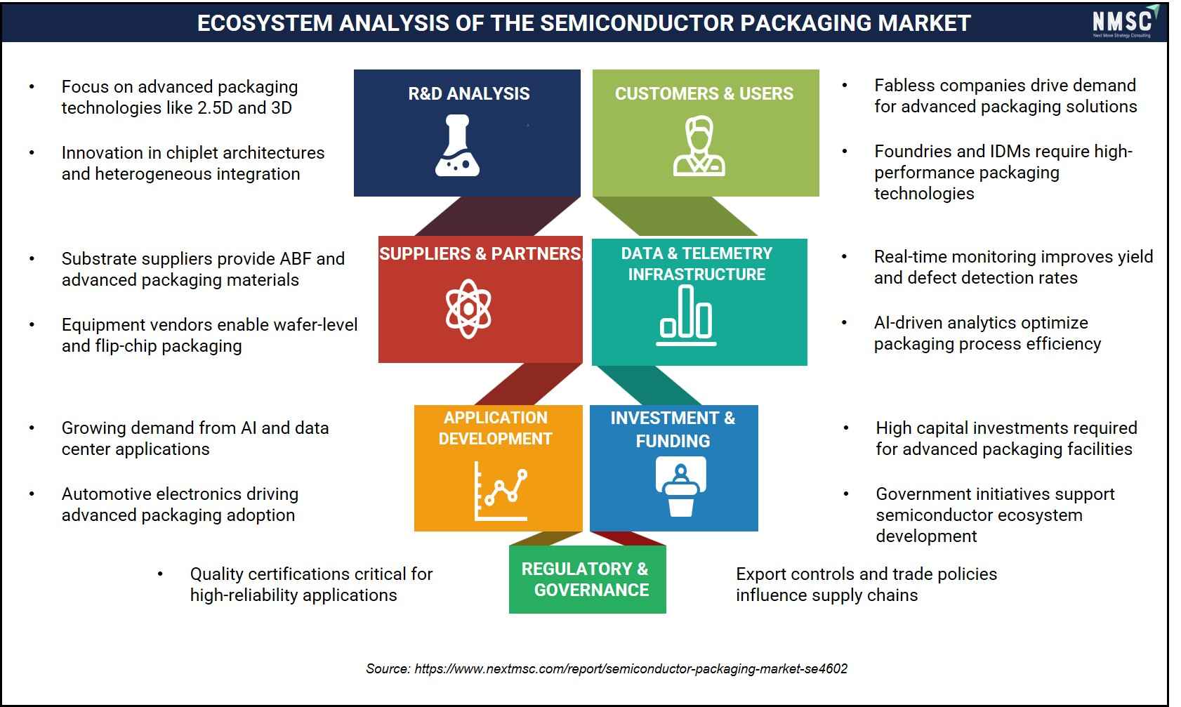
Based on our evaluation of the semiconductor packaging market ecosystem, we noticed that innovation in advanced packaging technologies such as 2.5D/3D integration, chiplet architectures, and wafer-level packaging continue to strengthen market development. Fabless companies, foundries, and IDMs are increasingly demanding high-performance packaging solutions to support AI processors, data center infrastructure, and automotive electronics. In addition, substrate suppliers and equipment manufacturers play a critical role in enabling advanced packaging capabilities and improving process efficiency. Moreover, increasing investments in semiconductor infrastructure, combined with supportive government initiatives and evolving trade policies, continue to shape global chip packaging solutions supply chains and long-term industry competitiveness.
What Are the Key Market Drivers, Breakthroughs, and Investment Opportunities that will Shape the Semiconductor Packaging Market in the Next Decade?
Growth Catalyst & Risk Assessment Matrix
|
Drivers / Trends / Restraints |
(+/–) % Impact on CAGR Forecast |
Geographic Relevance |
Impact Timeline |
|
Rising demand for AI processors, high-performance computing (HPC), and data center infrastructure accelerating adoption of advanced semiconductor packaging technologies |
+1.5% |
North America, Asia-Pacific (China, Taiwan, South Korea), Europe |
Medium to long-term (3–7 years) |
|
Increasing automotive electrification and growing adoption of SiC and GaN power semiconductors driving demand for thermally efficient and high-reliability packaging solutions |
+1.2% |
Europe (Germany), Asia-Pacific (Japan, China), North America |
Medium term (2–5 years) |
|
Transition toward chiplet architectures and heterogeneous integration increasing demand for high-density interconnects, advanced substrates, and 2.5D/3D packaging technologies |
+1.3% |
North America, Taiwan, South Korea, Europe |
Medium to long-term (3–6 years) |
|
Expansion of advanced packaging ecosystems and OSAT capacity investments strengthening scalability, manufacturing capabilities, and semiconductor supply chain resilience |
+1.0% |
Asia-Pacific, North America, Southeast Asia (India, Vietnam) |
Medium term (2–5 years) |
|
High capital expenditure requirements and increasing infrastructure complexity limiting advanced packaging expansion and entry of smaller market participants |
–1.2% |
Global (especially emerging markets) |
Short to medium term (1–4 years) |
Based on our evaluation of global semiconductor value chains and packaging ecosystems, we assessed that the semiconductor packaging market is experiencing strong structural growth, driven by increasing chip complexity, rising demand for AI and high-performance computing, and the shift toward advanced integration technologies. Our interactions with semiconductor manufacturers, OSAT providers, and chip designers indicate that packaging is no longer treated as a backend process but rather as a strategic enabler of performance and system level integration.
Simultaneously, advancements in chiplet architectures, heterogeneous integration, and 2.5D/3D packaging are enhancing interconnect density and thermal efficiency, particularly in data intensive applications. Additionally, our assessment of recent deployments shows that early stage co design between chip architecture and packaging layers improves scalability and accelerates time to market. However, increasing design complexity and the need for advanced substrates continue to influence cost structures. At the same time, stronger collaboration across foundries, OSAT providers, and material suppliers is improving ecosystem efficiency. Consequently, innovations in substrates and hybrid bonding are enabling scalable, high performance packaging solutions, reinforcing the role of packaging in next generation computing and AI driven applications.
Growth Drivers:
How Is AI Driven Memory Demand Accelerating Advanced Semiconductor Packaging Adoption?
Based on our evaluation of AI infrastructure deployments and memory supply chains, we observed that the rapid expansion of high bandwidth memory (HBM), including HBM3e and emerging HBM4, is significantly accelerating demand for advanced semiconductor packaging. Through our interactions with chip architects and packaging specialists, we identified that AI workloads require ultra-high bandwidth, low latency, and efficient power delivery, which conventional packaging architectures struggle to support. According to the U.S. Department of Commerce, the CHIPS National Advanced Packaging Manufacturing Program (NAPMP) finalized USD 1.4 billion in award funding in 2025 to strengthen advanced packaging capabilities and support large-scale semiconductor manufacturing in the United States. Moreover, 3D stacking and through silicon via (TSV) technologies are enabling vertical memory integration, allowing closer proximity between compute and memory units. This architectural shift reduces signal delay and improves data throughput in AI accelerators and data centre processors. In addition, packaging solutions optimized for compute memory co integration consistently deliver higher efficiency and performance scalability. As a result, AI driven memory demand is positioning advanced packaging as a critical foundation for next generation semiconductor performance.
How Is Automotive Electrification Driving Demand for High Performance Packaging Solutions?
Through our engagement with automotive OEMs and semiconductor suppliers, we observed that the transition toward electric vehicles and high voltage (800V) architectures is significantly increasing the need for advanced semiconductor packaging. Our interactions indicate that next generation power devices based on silicon carbide (SiC) and gallium nitride (GaN) operate under extreme thermal and electrical conditions, requiring packaging solutions that ensure stability and long-term reliability. According to Infineon Technologies, 2025, the company achieved a major milestone in 200 mm silicon carbide (SiC) production, enabling scalable, high-volume manufacturing of power semiconductors for electric vehicles. This advancement reflects growing EV-driven demand for high-performance semiconductor devices, which in turn requires robust and thermally efficient packaging technologies for reliable operation. Furthermore, packaging directly influences heat dissipation, power density, and operational durability, particularly in EV powertrains and fast charging systems. At the same time, increasing integration of electronic control units is driving demand for compact and high-efficiency packaging formats. In our evaluation of industry developments, advanced packaging techniques that enhance thermal performance and electrical efficiency are gaining strong adoption. Consequently, automotive electrification is reinforcing the importance of robust, high reliability integrated circuit packaging solutions.
Growth Inhibitor:
How Is High Capital Expenditure Limiting Advanced Semiconductor Packaging Market Expansion?
Based on our assessment of semiconductor manufacturing investments and packaging infrastructure requirements, we observed that high capital expenditure remains a significant constraint for the expansion of advanced packaging capabilities. According to the European Commission in 2026, the European Chips Act mobilised more than USD 91 billion in semiconductor-related investments across design, pilot lines, packaging, and manufacturing activities. This reflects the substantial infrastructure and capital requirements associated with expanding advanced semiconductor packaging and semiconductor manufacturing capabilities across Europe. This highlights the extremely high capital intensity required to scale advanced packaging infrastructure, reinforcing how significant financial commitments and long investment cycles act as a constraint on broader industry participation and capacity expansion. Through our interactions with OSAT providers and equipment manufacturers, we identified that setting up 2.5D and 3D packaging lines requires substantial investment in cleanroom facilities, advanced lithography systems, and precision bonding equipment. Moreover, these high upfront costs create strong entry barriers, particularly for smaller and mid-sized players, limiting their ability to scale advanced packaging capabilities. In addition, continuous technology upgrades further increase capital intensity, extending payback periods and impacting investment decisions. As a result, this cost burden slows capacity expansion, restricts broader ecosystem participation, and delays the pace of advanced packaging adoption across the market.
Growth Opportunity:
How Are Medical and Wearable Applications Creating Opportunities for SiP Packaging Innovation?
From our evaluation of emerging application segments, we observed that system in package (SiP) technology is unlocking significant opportunities in medical devices and wearable electronics. Our interactions with device manufacturers and technology developers indicate that applications such as continuous glucose monitors, smart wearables, and biosensors require highly miniaturised, flexible, and biocompatible packaging solutions. According to the World Health Organisation, there are an estimated 2 million different kinds of medical devices across more than 7,000 generic device groups worldwide, highlighting the expanding ecosystem of connected diagnostic, monitoring, and wearable healthcare devices that increasingly require compact semiconductor integration and advanced SIP-based packaging solutions. This demonstrates the increasing reliance on highly integrated and miniaturised semiconductor packaging technologies to support multi-functional wearable devices. In addition, SiP enables the integration of multiple components within compact form factors, supporting continuous monitoring, real-time data processing, and improved device functionality. At the same time, growing demand for personalised healthcare solutions is accelerating innovation in low-power, high-reliability packaging architectures. From our assessment of development pipelines, solutions that combine miniaturisation with durability and user comfort are gaining strong traction. Consequently, medical and wearable applications are emerging as a semiconductor application area driving next-generation semiconductor packaging innovation.
Price Point Analysis of the Semiconductor Packaging Market
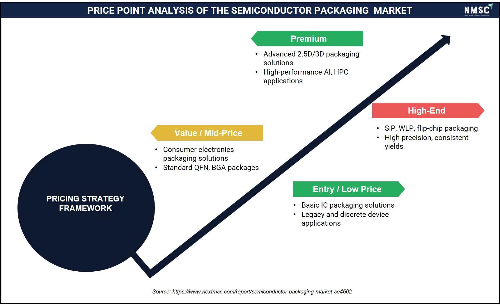
Based on our evaluation of the semiconductor packaging market, we noticed a clear pricing stratification driven by technology complexity and performance requirements. While entry level and mid-price segments cater to standard and high-volume consumer applications, high-end and premium tiers are dominated by advanced packaging solutions such as SiP, WLP, and 2.5D/3D architectures for AI and HPC use cases. Consequently, increasing demand for high performance computing and miniaturization is steadily shifting value toward premium offerings, reinforcing a technology led pricing hierarchy across the market.
How Is the Semiconductor Packaging Market Segmented in This Report, And What Are the Key Insights from the Segmentation Analysis?
Market Highlights & Strategic Insights – Semiconductor Packaging Market:
|
Segments |
Key Takeaways |
|
Packaging Technology |
Wire bond packaging dominates due to its cost efficiency and widespread use in analog and legacy devices. Flip chip gains strong traction driven by high-performance and high I/O requirements. Wafer level packaging expands with increasing demand for miniaturized and thin devices. 2.5D and 3D packaging emerge as key enablers for advanced computing, while embedded die packaging supports higher integration and compact designs. |
|
Package Type |
Grid array packages dominate due to their reliability and broad adoption in computing and consumer electronics. Flat no lead and flat leaded packages remain widely used in cost-sensitive and space-constrained applications. Chip scale packages gain traction with device miniaturization trends. Power packages expand with rising demand from electric vehicles and power electronics, while advanced and near chip scale formats support high-density applications. |
|
Substrate Type |
Organic substrates dominate the semiconductor packaging market, supported by their cost-performance balance and compatibility with advanced packaging. ABF substrates play a critical role in high-performance processors and networking devices. Silicon substrates gain traction in interposer-based packaging, while ceramic substrates support high-reliability and high-temperature applications. Glass substrates emerge as a next-generation option for improved performance and stability. |
|
End Use Industry |
Consumer electronics dominates demand, driven by high-volume production of smartphones, wearables, and computing devices. Data center and high-performance computing gain strong momentum with increasing deployment of AI accelerators and GPUs. Automotive expands rapidly with electric vehicles and ADAS adoption, while telecom, industrial, medical, and aerospace sectors support steady demand with reliability-focused applications. |
By Packaging Technology Insights
Which Packaging Technologies Drive Growth in the Semiconductor Packaging Market?
Based on our analysis of packaging technology adoption and industry engagement across semiconductor value chains, we segment the semiconductor packaging market into wire bond packaging, flip chip packaging, wafer level packaging, 2.5D packaging, 3D packaging, and embedded die packaging.
Through our interactions with industry participants and insights drawn from deployment trends, we observed that wire bond packaging continues to dominate, driven by its cost efficiency and extensive use in analog, discrete, and legacy devices. However, we identify that flip chip packaging gains strong traction as performance and I/O density requirements increase. At the same time, we note that wafer level packaging expands steadily, supported by growing demand for compact and thin semiconductor designs. Furthermore, we find that 2.5D and 3D packaging emerge as key growth drivers, particularly in AI and high-performance computing applications. Meanwhile, embedded die packaging supports increasing integration requirements in space-constrained designs. In conclusion, while conventional technologies sustain volume demand, advanced packaging technologies drive future growth and innovation.
By Package Type Insights
How Do Package Types Influence in the Semiconductor Packaging Market Demand?
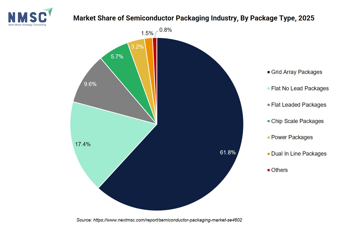
Based on our package-level assessment and engagement with packaging stakeholders, we categorized the semiconductor packaging market into grid array packages, flat no lead packages, flat leaded packages, chip scale packages, power packages, dual in line packages, and others.
Through our analysis and insights drawn from application trends, we found that grid array packages dominate, supported by their reliability and widespread use in computing and consumer electronics. In addition, we identify that flat no lead and flat leaded packages remain widely adopted in cost-sensitive and space-constrained applications. Meanwhile, we note that chip scale packages gain traction as device miniaturization accelerates across smartphones and wearable devices. Furthermore, we find that power packages expand with increasing demand from electric vehicles and power electronics. At the same time, advanced and near chip scale formats support high-density and performance-driven applications. As a result, traditional package types maintain stability, while miniaturized and advanced formats contribute to incremental growth.
By End Use Industry Insights
Which End Use Industries Drive Demand in the Semiconductor Packaging Market?
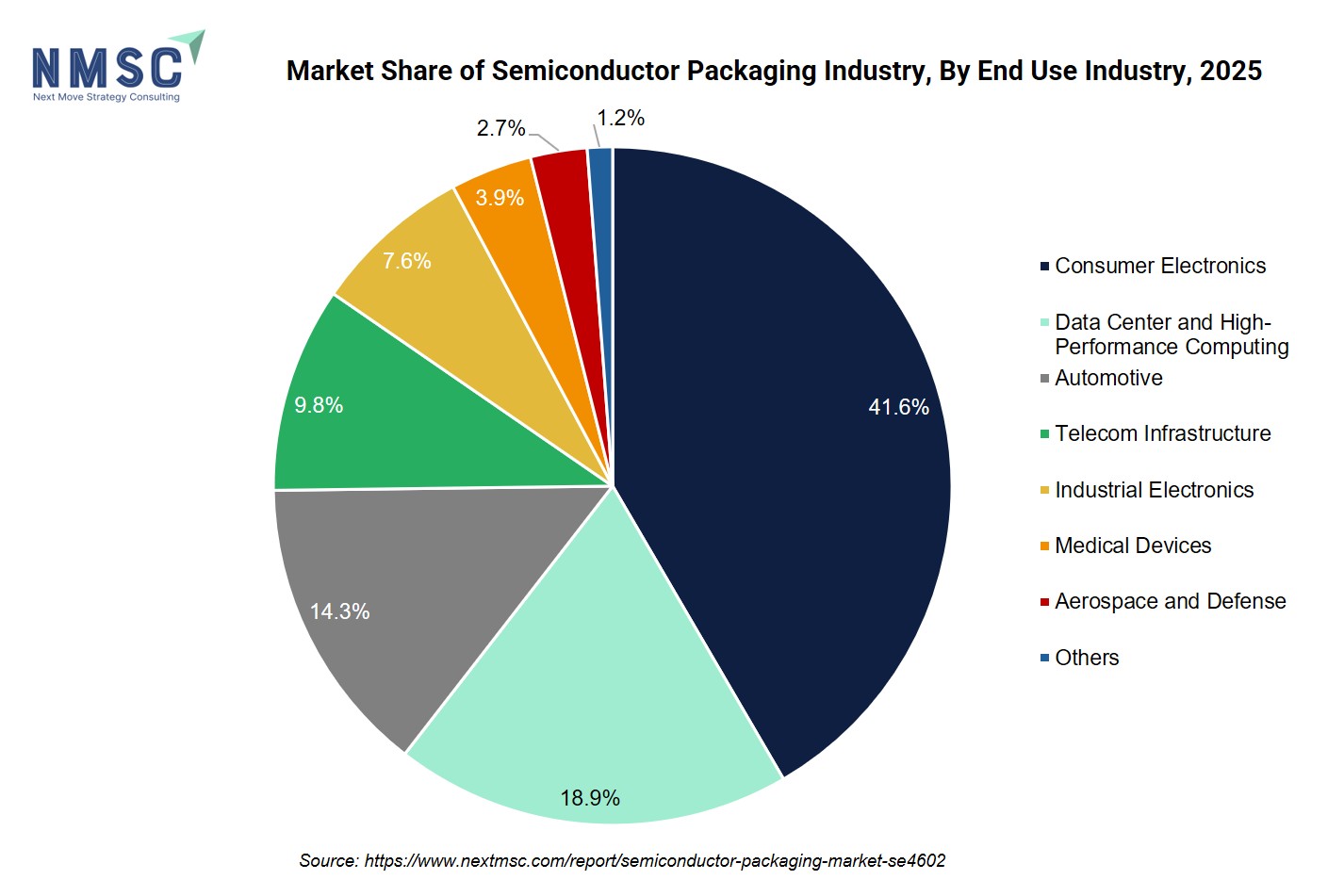
Based on our analysis and industry engagement, we segment the semiconductor packaging market into consumer electronics, automotive, data center and high-performance computing, telecom infrastructure, industrial electronics, medical devices, aerospace and defense, and others.
Through our interactions and insights drawn from demand patterns, we noticed that consumer electronics dominate, driven by high-volume production of smartphones, wearables, and computing devices. However, we identify that data center and high-performance computing emerge as the fastest-growing segments, supported by increasing deployment of AI accelerators and advanced processors. In addition, we note that the automotive sector gains strong momentum with the rise of electric vehicles and advanced driver assistance systems. Meanwhile, telecom infrastructure continues to expand with 5G and networking demand. At the same time, industrial, medical, and aerospace sectors maintain steady adoption, driven by reliability and precision requirements. This contributes to a gradual shift in growth toward high-performance and automotive-driven applications, while consumer electronics continues to anchor overall volume demand.
Regional Outlook:
Geographic Performance Snapshot:
|
Geography |
Key Takeaways |
|
North America |
North America demonstrates strong activity in the semiconductor packaging market, driven by increasing deployment of AI processors, high-performance computing systems, and advanced automotive electronics. Companies such as Intel Corporation continue investing in advanced packaging technologies, including chiplet integration and 2.5D/3D packaging. In addition, growing focus on domestic semiconductor manufacturing and packaging capabilities continues strengthening regional supply chain resilience. |
|
Europe |
Europe shows steady demand in the semiconductor packaging market across automotive electronics, industrial automation systems, and power semiconductor applications. The region increasingly emphasizes thermally stable and energy-efficient semiconductor packaging technologies, particularly for electric vehicles and industrial equipment. Furthermore, expanding adoption of power semiconductors and advanced automotive electronics continues supporting packaging innovation across European markets. |
|
Asia Pacific |
Asia Pacific represents a major manufacturing centre in the semiconductor packaging market due to its integrated semiconductor supply chains and extensive electronics production networks. Strong consumer electronics manufacturing and increasing deployment of AI servers, data centre hardware, and automotive electronics continue driving semiconductor packaging demand across the region. Moreover, major OSAT providers and semiconductor foundries continue expanding advanced packaging capacity throughout Asia Pacific. |
|
Latin America |
Latin America is witnessing gradual expansion in semiconductor packaging activities, influenced by increasing electronics manufacturing and participation in global electronics supply chains. Demand remains associated with consumer electronics, industrial equipment, and automotive electronics applications across regional markets. In addition, ongoing industrial development continues supporting semiconductor assembly and packaging operations throughout the region. |
|
Middle East & Africa |
The Middle East & Africa region is experiencing gradual development in semiconductor packaging activities, driven by investments in electronics manufacturing, telecom infrastructure, and industrial digitalization initiatives. Increasing deployment of connected technologies and electronic systems continues contributing to semiconductor demand across the region. Expanding infrastructure projects and industrial modernization efforts also continue supporting growth in the semiconductor packaging market. |
The semiconductor packaging market is geographically studied across North America, Europe, Asia Pacific, Latin America and Middle East & Africa and each region is further studied across countries.
Semiconductor Packaging Market in North America
From our regional assessments, we identified that North America’s semiconductor packaging market continues to evolve with increasing adoption of AI processors, high-performance computing systems, and advanced automotive electronics. The region demonstrates a growing transition toward advanced packaging technologies, including chiplet integration and 2.5D/3D architectures, as semiconductor performance and bandwidth requirements continue to increase. Moreover, the presence of integrated semiconductor companies such as Intel Corporation, along with collaboration across design, fabrication, and packaging operations, continues to strengthen advanced packaging development across the region. In addition, ongoing investments in domestic semiconductor manufacturing and packaging infrastructure contribute to expanding advanced packaging capabilities. As semiconductor companies continue expanding AI processors, advanced computing systems, and chiplet-based architectures, demand for high-density and advanced semiconductor packaging technologies continues to increase across North America.
Semiconductor Packaging Market in the United States
In the United States, the semiconductor packaging market is undergoing a transition toward design-integrated packaging, where packaging increasingly functions as a core component of semiconductor performance optimization. Based on our analysis of semiconductor deployment trends, we observed that demand is primarily associated with AI workloads, hyperscale data centres, and next-generation processors. Furthermore, companies such as Intel Corporation continue expanding advanced packaging capabilities, particularly across chiplet-based architectures and high-density interconnect technologies. At the same time, coordination between fabless companies, foundries, and OSAT providers continues to accelerate packaging development and semiconductor integration processes. This increases adoption of advanced semiconductor packaging technologies across AI accelerators, high-bandwidth computing systems, and next-generation processor architectures in the United States.
Semiconductor Packaging Market in Canada
The semiconductor packaging market in Canada is a steadily evolving environment, where market activity aligns with its participation in the broader electronics and semiconductor value chain. Based on our assessment of industrial electronics and telecom infrastructure developments, we identified that demand is associated with automotive electronics, industrial systems, and communication equipment applications. In addition, the country continues leveraging capabilities in advanced materials, semiconductor research, and precision engineering to support development of specialized semiconductor packaging solutions. Compared with the United States, the Canadian market places greater emphasis on reliability-oriented packaging applications across industrial and telecom environments. As adoption of industrial automation systems, connected infrastructure, and automotive electronics continues to increase, demand for semiconductor packaging solutions also expands across Canada.
Semiconductor Packaging Market in Europe
The European semiconductor packaging market evolves as a quality centric and compliance driven landscape, where performance standards and regulatory alignment shape adoption patterns. Based on our regional analysis of automotive and industrial value chains, we identified that demand is primarily anchored in electric vehicles, industrial automation, and power electronics. Moreover, stringent EU regulations around energy efficiency and product reliability elevate the need for thermally stable and durable packaging solutions. Across key economies, adoption patterns vary, with Germany emphasizing engineering precision, while Southern Europe prioritizes flexible and application specific packaging approaches. In addition, strong collaboration between semiconductor firms, equipment providers, and industrial manufacturers strengthens deployment efficiency. These dynamics enhance vendor credibility through higher qualification standards, stronger system reliability, and longer-term contracts, positioning Europe as a high trust, performance-oriented semiconductor packaging region.
Semiconductor Packaging Market in the United Kingdom
Based on our interaction with ecosystem participants, we noticed that the United Kingdom’s semiconductor packaging market is steadily transitioning toward innovation led and application specific demand, supported by advancements in telecom and data infrastructure. The growing deployment of high-speed communication systems and edge computing continues to drive the need for compact, high performance packaging solutions. Furthermore, collaboration between design firms, research institutions, and packaging providers accelerates early-stage innovation and commercialization. The market also reflects a preference for scalable and adaptable packaging formats, particularly those supporting miniaturization and high data throughput. In addition, procurement decisions increasingly consider lifecycle support and system transparency, encouraging partnerships with technically robust providers. As a result, the UK strengthens its position in specialized and innovation driven semiconductor packaging applications.
Semiconductor Packaging Market in Germany
Germany’s semiconductor packaging market reflects an engineering-intensive and industrially integrated environment, closely aligned with the country’s automotive and industrial manufacturing sectors. Based on our assessment of industrial semiconductor applications, we observed that demand remains associated with automotive electronics, power semiconductors, factory automation systems, and industrial control equipment. Furthermore, stringent performance and thermal reliability requirements continue increasing adoption of durable and application-specific semiconductor packaging technologies across industrial environments. Meanwhile, collaboration between semiconductor manufacturers, industrial equipment providers, and automotive electronics companies continues supporting deployment of high-reliability semiconductor packaging solutions. Ultimately, expanding electric vehicle production and increasing industrial automation activities continue strengthening semiconductor packaging demand across Germany.
Semiconductor Packaging Market in France
Through our analysis of regional industry dynamics, we identified that France’s semiconductor packaging market is expanding with a strong focus on reliability driven and mission critical applications, particularly across aerospace, defense, and industrial electronics. Packaging solutions that ensure thermal stability, traceability, and compliance continue to gain higher adoption. Additionally, national emphasis on technological sovereignty and industrial modernization supports increased investments in semiconductor capabilities. Collaboration between research institutions, semiconductor firms, and system developers further strengthens innovation in advanced materials and packaging techniques. In addition, buyers prioritize system safety and long-term performance, favouring solution providers with proven technical expertise. As a result, France continues to build a specialized and high reliability semiconductor packaging ecosystem.
Semiconductor Packaging Market in Italy
Italy’s semiconductor packaging market reflects a progressive shift toward flexible and application driven solutions, supported by ongoing industrial modernization. Through our analysis of regional supply chains, we identified increasing demand across automotive components, consumer electronics, and industrial equipment. Moreover, fragmented manufacturing infrastructure creates a need for adaptable and modular packaging approaches, enabling compatibility across diverse applications. Government initiatives promoting efficiency and digital transformation further support adoption. In addition, solution providers offering customized deployment and localized technical support achieve stronger market penetration compared to standardized offerings. Therefore, Italy continues to evolve as a practical and customization focused market, where flexibility and cost performance balance drive packaging adoption.
Semiconductor Packaging Market in Spain
Spain is witnessing gradual expansion in semiconductor packaging demand, influenced by increasing electronics deployment and industrial digitalization activities. From our engagement with regional distributors and technology providers, we found that demand remains associated with automotive electronics, industrial control systems, and consumer electronic devices. Furthermore, growing emphasis on energy-efficient electronic systems and industrial automation continues encouraging adoption of advanced semiconductor packaging technologies across the country. While operational efficiency remains an important consideration, buyers increasingly prioritize semiconductor packaging solutions that provide stable performance and integration flexibility. Meanwhile, industrial and manufacturing hubs continue recording increasing semiconductor usage across electronics applications. As a result, expanding deployment of industrial electronics and connected systems continues strengthening semiconductor packaging demand across Spain.
Semiconductor Packaging Market in the Nordics
The Nordic semiconductor packaging landscape, including Sweden, Finland, and Norway, reflects a highly mature, quality first adoption environment, where precision, sustainability, and long-term performance define market expectations. Through our interaction with regional industry participants, we identified that demand is closely aligned with advanced electronics, telecom infrastructure, and industrial applications. Simultaneously, strong digital maturity and early adoption of automation technologies support the uptake of advanced and reliable packaging solutions, particularly those offering thermal efficiency and durability. Buyers consistently prefer environmentally sustainable materials, energy efficient processes, and transparent lifecycle support. In addition, collaboration with research institutions and local technology partners strengthens innovation capabilities. As a result, vendors focusing on high performance packaging, sustainability compliance, and long-term service engagement secure stronger positioning and repeat business across the Nordic semiconductor ecosystem.
Semiconductor Packaging Market in Asia Pacific
Our regional supply chain analysis indicates that Asia-Pacific represents a major semiconductor packaging manufacturing hub due to its integrated semiconductor supply chains and extensive electronics production networks. Strong demand across consumer electronics, data centres, automotive electronics, and advanced computing applications continues to enable large-scale semiconductor packaging operations throughout the region. While China emphasises manufacturing scale and cost efficiency, Japan focuses on precision-oriented semiconductor applications, whereas South Korea accelerates the deployment of advanced packaging technologies. Additionally, major OSAT providers and semiconductor foundries such as TSMC continue expanding advanced packaging capabilities across Asia-Pacific. Consequently, rising semiconductor manufacturing activity and broader deployment of advanced electronic systems continue to reinforce semiconductor packaging demand across the region.
Semiconductor Packaging Market in China
China represents a significant semiconductor packaging manufacturing market within Asia-Pacific, influenced by extensive electronics production capabilities and expanding semiconductor supply chain activities. Based on our assessment of regional manufacturing operations, we observed that demand remains associated with consumer electronics, telecom infrastructure, AI hardware, and data processing applications. In addition, domestic semiconductor companies continue expanding assembly, testing, and packaging capabilities to strengthen local semiconductor production activities. While cost-efficient manufacturing remains an important factor, increasing investments in semiconductor infrastructure and packaging technologies continue to improve operational capabilities across the country. Moreover, integration between electronics manufacturing and semiconductor packaging operations continues to support large-scale production activities. Consequently, expanding semiconductor manufacturing capacity and increasing deployment of advanced electronic systems continue to reinforce semiconductor packaging demand across China.
Semiconductor Packaging Market in Japan
Based on our field-level assessment of industrial dynamics, we observed that Japan’s semiconductor packaging market continues evolving through reliability-oriented and precision-focused semiconductor manufacturing practices. Demand remains concentrated in automotive electronics, industrial systems, and high-end consumer electronic devices, where operational consistency and thermal reliability remain critical requirements. At the same time, Japanese semiconductor manufacturers continue emphasizing advanced materials, packaging precision, and stable long-term system performance across semiconductor applications. The market also benefits from collaboration between semiconductor companies, equipment manufacturers, and research institutions, supporting ongoing advancements in semiconductor packaging materials and integration technologies. Ultimately, increasing deployment of automotive electronics and industrial semiconductor systems continues driving demand for high-reliability semiconductor packaging technologies across Japan.
Semiconductor Packaging Market in India
India’s semiconductor packaging market is evolving as an expanding semiconductor manufacturing and electronics assembly landscape, driven by increasing electronics consumption and policy-backed semiconductor initiatives. Based on our interactions with industry participants, we found that demand is primarily associated with consumer electronics, telecom infrastructure, and automotive electronics applications. Simultaneously, government programs supporting domestic semiconductor manufacturing and supply chain development continue strengthening assembly, testing, and packaging (ATP) capabilities across the country. In addition, cost competitiveness and availability of skilled engineering talent continue improving the country’s semiconductor manufacturing environment. Vendors focusing on localized semiconductor packaging operations, scalable manufacturing capabilities, and industry partnerships continue expanding market presence across India. Thus, increasing semiconductor manufacturing investments and expanding electronics production continue accelerating semiconductor packaging activities throughout the country.
Semiconductor Packaging Market in South Korea
Based on our analysis of semiconductor manufacturing activities, we identified that South Korea represents an advanced semiconductor packaging market associated with memory semiconductors, AI processors, and high-end consumer electronics applications. Demand continues increasing across high-bandwidth memory (HBM), advanced computing systems, and data centre hardware requiring high-density semiconductor packaging technologies. At the same time, vertically integrated semiconductor companies such as Samsung Electronics continue strengthening advanced packaging capabilities through ongoing technology development and manufacturing integration. Furthermore, collaboration between semiconductor manufacturers and equipment providers continues supporting deployment of advanced packaging architectures, including 3D stacking technologies. As a result, increasing deployment of AI processors and memory-intensive semiconductor applications continues accelerating semiconductor packaging activities across South Korea.
Semiconductor Packaging Market in Taiwan
Taiwan represents an important semiconductor packaging manufacturing market due to its established semiconductor fabrication ecosystem and advanced packaging capabilities. From our assessment of semiconductor supply chain activities, we observed that demand is primarily associated with high-performance computing processors, AI chips, networking equipment, and advanced logic semiconductors. In addition, semiconductor foundries and OSAT providers continue expanding packaging technologies such as CoWoS and integrated fan-out packaging to support increasing semiconductor complexity and bandwidth requirements. Meanwhile, close coordination between semiconductor design companies, foundries, and packaging providers continues improving packaging integration and production efficiency. Thus, increasing deployment of AI accelerators and advanced computing hardware continues to strengthen semiconductor packaging demand across Taiwan.
Semiconductor Packaging Market in Indonesia
Indonesia’s semiconductor packaging market is at an early yet gradually expanding stage, shaped by increasing electronics demand and improving industrial infrastructure. Based on our assessment of electronics manufacturing activities, we observed that semiconductor packaging operations remain concentrated in consumer electronics assembly and conventional packaging processes, particularly across major industrial and manufacturing zones. In addition, affordability and operational scalability continue to influence the adoption of cost-efficient semiconductor packaging solutions across the country. The market also benefits from collaboration between electronics manufacturers and local industry participants, supporting the gradual development of semiconductor assembly and packaging capabilities. Furthermore, government initiatives focused on industrial expansion and digitalization continue to strengthen electronics manufacturing activities. Consequently, rising electronics assembly activities and improving industrial capabilities continue to increase semiconductor packaging deployment across Indonesia.
Semiconductor Packaging Market in Australia
Through our analysis of regional semiconductor and electronics applications, we identified that Australia’s semiconductor packaging market reflects demand across industrial electronics, telecom infrastructure, defence electronics, and specialised semiconductor applications. Moreover, industries operating in remote and industrial environments continue emphasising reliable semiconductor packaging solutions capable of supporting stable system performance and extended operational lifecycles. Buyers also increasingly prioritise testing, validation, and lifecycle management capabilities when selecting semiconductor packaging technologies for industrial and communication systems. In addition, collaboration with global semiconductor companies continues to improve access to advanced packaging technologies and technical expertise across the country. Ultimately, increasing deployment of industrial automation systems and communication infrastructure continues to support semiconductor packaging demand across Australia.
Semiconductor Packaging Market in Latin America
The semiconductor packaging market in Latin America is developing steadily, with Brazil representing a significant regional electronics manufacturing market. Based on our assessment of regional electronics supply chains, we observed that demand remains associated with consumer electronics, industrial equipment, and automotive electronics applications. In addition, semiconductor packaging activities across the region continue focusing on assembly, testing, and conventional packaging processes, while gradual investments improve manufacturing and operational capabilities. Although pricing considerations remain important across several regional markets, increasing participation in global electronics manufacturing networks continues supporting semiconductor packaging activities. Consequently, expanding electronics production and industrial automation applications continue creating demand for semiconductor assembly and packaging operations across Latin America..
Semiconductor Packaging Market in the Middle East & Africa
Based on our assessment of regional electronics and industrial ecosystems, we observed that the Middle East & Africa semiconductor packaging market is evolving across varying stages of industrial development. The Middle East, particularly Gulf economies, demonstrates increasing semiconductor demand associated with telecom infrastructure, smart technologies, industrial automation, and digital infrastructure projects. In contrast, several African markets remain focused on electronics assembly and conventional semiconductor packaging activities at an early development stage. In addition, infrastructure expansion and increasing adoption of connected electronic systems continue supporting semiconductor demand across the region. Market participants increasingly focus on scalable and application-specific semiconductor packaging solutions aligned with regional industrial and electronics requirements. Ultimately, expanding digital infrastructure and industrial modernization initiatives continue supporting gradual semiconductor packaging adoption across the Middle East & Africa.
Porter’s Five Forces Analysis of the Semiconductor Packaging Market
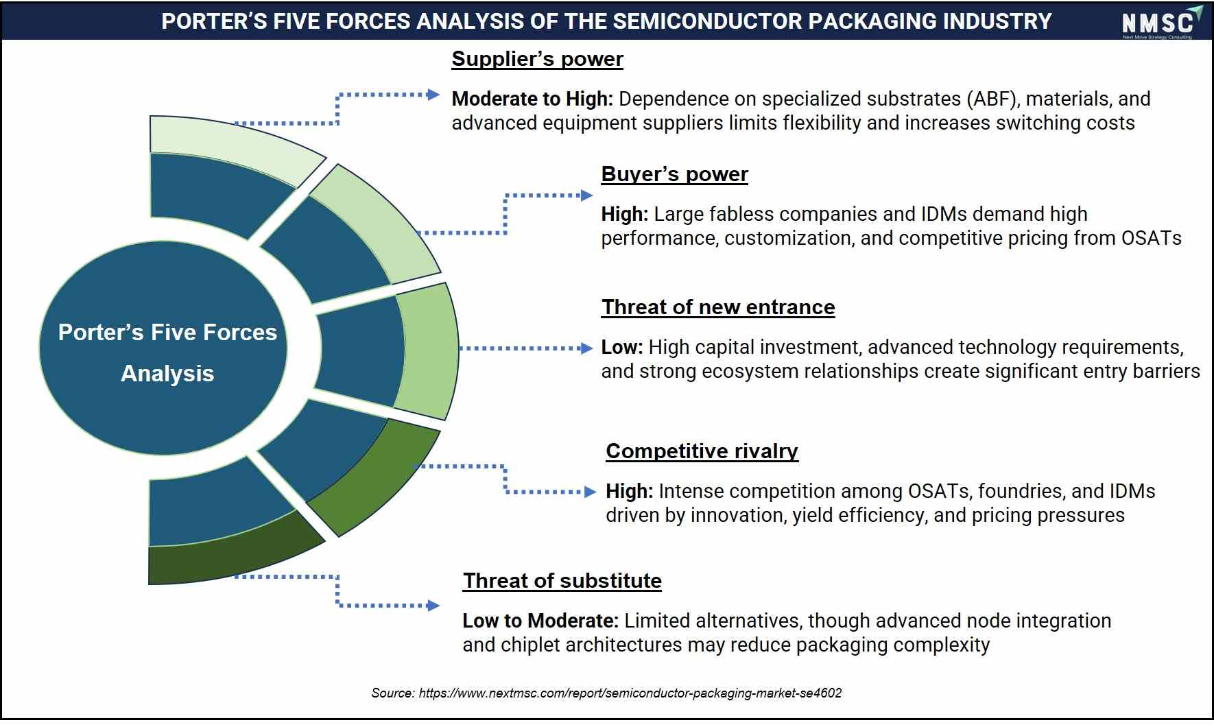
Based on our evaluation of the semiconductor packaging industry, we observed that high entry barriers and strong supplier dependencies shape the competitive landscape, while large fabless companies and IDMs exert significant buyer power. At the same time, intense rivalry among OSATs and continuous innovation requirements drive competition, even as limited substitutes reinforce the critical role of advanced packaging technologies in enabling next generation semiconductor performance.
Competitive Landscape
Competitive Dynamics & M&A Landscape:
|
Key Takeaways |
|
The semiconductor packaging market is shaped by large integrated device manufacturers and leading foundries alongside specialized OSAT and discrete semiconductor players. Major companies such as Intel Corporation, Samsung Electronics, Taiwan Semiconductor Manufacturing Company Limited, Texas Instruments, and Infineon Technologies leverage advanced packaging capabilities, vertically integrated manufacturing, and strong R&D investments to maintain market leadership. Meanwhile, companies including Amkor Technology, Nexperia, Vishay Intertechnology, Diodes Incorporated, and ams OSRAM AG strengthen competition through specialized packaging solutions, discrete semiconductor expertise, and application specific innovations. |
|
Companies increasingly prioritize advanced packaging technologies such as heterogeneous integration, 2.5D/3D packaging, and system in package (SiP) solutions to support high performance computing, AI, and automotive applications. Additionally, miniaturization, power efficiency optimization, and high-density interconnect innovations continue shaping product development. Companies also expand outsourced semiconductor assembly and test (OSAT) partnerships and invest in regional packaging facilities to enhance supply chain resilience and meet growing demand. |
|
Recent consolidation also reflects efforts to strengthen technological capabilities and geographic presence across the semiconductor packaging market. Strategic partnerships and long-term supply agreements particularly between IDMs and OSAT providers enable companies to improve manufacturing flexibility, scale advanced packaging capacity, and address increasing complexity in chip design. As a result, the market witnesses stronger alignment between design, fabrication, and packaging processes, enhancing performance efficiency and accelerating time to market across end use industries. |
Which Companies Dominate the Semiconductor Packaging Market and How Do They Compete?
Based on our market analysis, we found that the semiconductor packaging market is dominated by large integrated device manufacturers (IDMs) and leading foundries alongside specialized outsourced semiconductor assembly and test (OSAT) providers. Companies such as Intel Corporation, Samsung Electronics, and Taiwan Semiconductor Manufacturing Company Limited consistently lead in advanced packaging deployments where performance optimization, chiplet integration, and high-bandwidth requirements are critical decision factors. From our assessment, we found that these players are frequently selected for high-performance computing, AI accelerators, and data center applications due to their capabilities in 2.5D/3D packaging, heterogeneous integration, and tight design-manufacturing alignment. Meanwhile, Amkor Technology strengthens its position as a leading OSAT provider by offering scalable, cost-efficient packaging solutions across consumer electronics, automotive, and industrial segments. Competition at this level is primarily driven by advanced packaging capabilities, yield optimization, and the ability to support next-generation semiconductor architectures.
Market Dominated by Semiconductor Packaging Giants and Specialists
From our market observation, we found that the competitive landscape is further shaped by IDM and application-specific semiconductor players such as Texas Instruments, Infineon Technologies, NXP Semiconductors, STMicroelectronics, and Renesas Electronics. Our analysis indicates that these companies gain traction through in-house and hybrid packaging models tailored to power electronics, automotive, and industrial applications, where reliability, thermal performance, and long product lifecycles are essential.
Additionally, players such as Nexperia, Vishay Intertechnology, Diodes Incorporated, and Littelfuse strengthen competition through discrete and power semiconductor packaging expertise, while memory-focused companies including Winbond Electronics and Macronix International focus on high-density and cost-efficient packaging for memory devices. In practice, large IDMs and foundries set performance benchmarks, while specialized players address application-specific requirements and cost-sensitive markets.
Innovation and Adaptability Drive Market Success
Innovation remains a core determinant of competitive advantage in the semiconductor packaging market, as identified through our assessment of technology roadmaps and industry deployments. Market leaders such as Intel Corporation, TSMC, and Samsung Electronics advance capabilities in chiplet architectures, 2.5D/3D integration, fan-out wafer-level packaging (FOWLP), and system-in-package (SiP) technologies. These innovations enable higher interconnect density, improved power efficiency, and reduced latency for next-generation applications. From our market analysis, we noticed that companies investing in heterogeneous integration, advanced substrates, and thermal management solutions are better positioned to support AI workloads, automotive electrification, and high-performance computing demands. Additionally, packaging is increasingly integrated into chip design strategies, making it a critical enabler of overall system performance rather than a backend process.
Market Players to Opt for Merger & Acquisition Strategies to Expand Their Presence
From our primary research, we evaluated that strategic partnerships and long-term supply agreements are emerging as key growth levers in the semiconductor packaging market. Collaborations between IDMs and OSAT providers, such as partnerships involving Infineon Technologies and Amkor Technology, focus on expanding packaging capacity, improving regional supply chain resilience, and addressing rising demand from automotive and industrial sectors. Our analysis indicates that companies increasingly invest in regional packaging facilities, particularly in Europe and Asia-Pacific, to mitigate supply chain risks and comply with localization strategies. Rather than focusing solely on scale, these initiatives prioritize advanced packaging capabilities, faster time-to-market, and improved integration with fabrication processes. As competition intensifies, partnerships, capacity expansion, and ecosystem collaboration continue to reshape the market by strengthening technological capabilities and global execution.
List of Key Semiconductor Packaging Companies
-
Intel Corporation
-
Taiwan Semiconductor Manufacturing Company Limited
-
Texas Instruments Incorporated
-
Infineon Technologies AG
-
NXP Semiconductors N.V.
-
Amkor Technology, Inc.
-
Vishay Intertechnology, Inc.
-
Diodes Incorporated
-
STMicroelectronics N.V.
-
Renesas Electronics Corporation
-
United Microelectronics Corporation
-
Winbond Electronics Corporation
-
Tongfu Microelectronics Co., Ltd.
-
Macronix International Co., Ltd.
-
Littelfuse, Inc.
-
Nexperia B.V.
-
Ampleon Netherlands B.V.
-
ams-OSRAM AG
What Are the Latest Key Industry Developments?
-
March 2026 – Intel confirmed the readiness of its Intel 18A process technology featuring RibbonFET and PowerVia architectures. The development supports next-generation AI and high-performance computing applications while strengthening advanced semiconductor integration capabilities.
-
February 2026 – Renesas Electronics Corporation signed a definitive agreement to transfer its timing business to SiTime Corporation in a transaction valued at approximately USD 1.5 billion in cash, alongside stock consideration. Additionally, both companies signed an MoU to develop integrated solutions combining SiTime’s MEMS resonators with Renesas MCUs and SoCs through bare-die co-packaging, supporting advanced semiconductor integration and device miniaturization.
-
October 2025 – NXP Semiconductors N.V. completed the acquisitions of Aviva Links for USD 243 million and Kinara, Inc. for USD 307 million, strengthening its automotive connectivity and AI-powered edge computing capabilities across automotive and industrial IoT applications.
Expert Insights

“ Rapid growth in compute requirements for system on chips (SoCs), artificial intelligence (AI) accelerators, and networking devices is pushing traditional semiconductor packaging to its limits….This evolution requires innovative packaging architectures to support expanded area, higher interconnect density, and enhanced power and thermal management to meet the needs of next-generation devices.”
- Mark Gardner, Vice President of Intel Corporation
“Statement made during an Intel Corporation discussion on advancements in semiconductor packaging and integration technologies.
Market Interpretation
The statement emphasized the increasing importance of advanced packaging in enabling multi-die integration and chiplet-based architectures. As demand for high-performance computing (HPC) and artificial intelligence (AI) applications rises, semiconductor companies are leveraging advanced packaging to overcome the physical and economic limitations of monolithic chip designs. This trend is accelerating the adoption of heterogeneous integration and reinforcing packaging as a key driver of innovation in the semiconductor industry.
What Are the Key Factors Influencing Investment Analysis & Opportunities in the Semiconductor Packaging Market?
Investment activity in the semiconductor packaging market is increasingly focused on advanced packaging technologies that support AI processors, high-performance computing, automotive electronics, and data center infrastructure. Through our market assessment, we observed that semiconductor companies are prioritizing investments in 2.5D/3D packaging, heterogeneous integration, chiplet architectures, and system-in-package (SiP) technologies to improve interconnect density, thermal efficiency, and overall chip performance.
In addition, semiconductor manufacturers and OSAT providers are expanding advanced packaging capacity and strengthening regional supply chain capabilities to support rising semiconductor demand and improve operational resilience. Moreover, investments are increasingly directed toward advanced substrates, thermal management technologies, wafer-level packaging, and hybrid bonding solutions to address growing performance and miniaturization requirements.
Consequently, rising adoption of AI accelerators, electric vehicles, and high-performance computing systems continues to create strong opportunities for advanced semiconductor packaging technologies, supporting long-term investment potential across the market.
Key Benefits for Stakeholders:
Next Move Strategy Consulting (NMSC) presents a comprehensive analysis of the semiconductor packaging market trends, covering historical developments from 2020 to 2025 and providing forward looking forecasts through 2035.
Our study evaluates the semiconductor packaging market at global, regional, and country levels, providing quantitative outlooks and insights into key growth drivers, challenges, technology shifts, and investment trends across major packaging segments.
From our observation, we found that the market delivers value across a broad stakeholder base. Investors benefit from strong demand driven by AI, HPC, and automotive applications, supported by capacity expansion and strategic partnerships. Companies such as Intel Corporation, Samsung Electronics, and TSMC strengthen confidence through advanced packaging capabilities and integrated models. Semiconductor manufacturers and OSAT providers, including Amkor Technology, benefit from performance optimization, outsourcing trends, and rising demand for scalable solutions. Overall, the market supports efficiency, innovation, and long-term growth across the semiconductor value chain.
|
Parameters |
Details |
|
Customization Scope |
Free customization (equivalent to up to 80 analyst working hours) after purchase. Addition or alteration to country, regional & segment scope. |
|
Pricing and Purchase Options |
Avail customized purchase options to meet your exact research needs. |
|
Approach |
In depth primary and secondary research; proprietary databases; rigorous quality control and validation measures. |
|
Analytical Tools |
Porter's Five Forces, SWOT, value chain, and Harvey ball analysis to assess competitive intensity, stakeholder roles, and relative impact of key factors. |
Semiconductor Packaging Market Key Segments
By Packaging Technology
-
Wire Bond Packaging
-
Leadframe-Based Packages
-
Substrate-Based Wire Bond
-
Multi-Chip Wire Bond
-
Discrete And Analog Packaging
-
-
Flip Chip Packaging
-
Flip Chip on Substrate
-
Flip Chip on Leadframe
-
Flip Chip Ball Grid Array
-
Wafer Bumping
-
-
Wafer Level Packaging
-
Fan In Wafer Level Packaging
-
Fan Out Wafer Level Packaging
-
Chip First Fan Out
-
Chip Last Fan Out
-
-
-
2.5D Packaging
-
Silicon Interposer Based
-
Organic Interposer Based
-
-
3D Packaging
-
Embedded Die Packaging
-
Embedded in Substrate
-
Embedded in PCB
-
Embedded Wafer Level
-
By Package Type
-
Grid Array Packages
-
Ball Grid Array
-
Micro Ball Grid Array
-
Land Grid Array
-
-
Flat No Lead Packages
-
Quad Flat
-
Dual Flat
-
Thin Flat
-
-
Flat Leaded Packages
-
Quad Flat Package
-
Thin Quad Flat Package
-
Small Outline Package
-
Shrink Small Outline Package
-
-
Chip Scale Packages
-
Wafer Level Chip Scale Package
-
Fan Out Chip Scale Package
-
Near Chip Scale Package
-
-
Power Packages
-
Dual-In-Line Packages
-
Plastic Dual in Line
-
Ceramic Dual in Line
-
-
Others
By Substrate Type
-
Leadframe
-
Copper Leadframe
-
Alloy Leadframe
-
-
Organic Substrate
-
BT Resin Substrate
-
ABF Substrate
-
High-Density Interconnect Substrate
-
-
Silicon Substrate
-
Active Interposer
-
Passive Interposer
-
-
Ceramic Substrate
-
Alumina
-
Aluminum Nitride
-
Others
-
-
Glass Substrate
By End Use Industry
-
Consumer Electronics
-
Smartphones
-
Tablets
-
Wearables
-
PCs and Laptops
-
Gaming Devices
-
-
Automotive
-
Advanced Driver Assistance Systems (ADAS)
-
Electric Vehicle Power Electronics
-
Infotainment Systems
-
Body Electronics
-
-
Data Center and High-Performance Computing
-
Central Processing Units
-
Graphics Processing Units
-
AI Accelerators
-
Memory Modules
-
-
Telecom Infrastructure
-
5G Base Stations
-
Optical Networking
-
Network Switches and Routers
-
-
Industrial Electronics
-
Factory Automation
-
Robotics
-
Power Control Systems
-
-
Medical Devices
-
Diagnostic Equipment
-
Imaging Systems
-
Wearable Medical Devices
-
-
Aerospace & Defense
-
Avionics
-
Radar Systems
-
Satellite Electronics
-
-
Others
Geographical Breakdown
-
North America: U.S., Canada, and Mexico.
-
Europe: UK, Germany, France, Italy, Spain, Sweden, Denmark, Finland, the Netherlands, and the Rest of Europe.
-
Asia Pacific: China, India, Japan, South Korea, Taiwan, Indonesia, Vietnam, Australia, Philippines, Malaysia and the rest of APAC.
-
Middle East & Africa (MEA): Saudi Arabia, UAE, Egypt, Israel, Turkey, Nigeria, South Africa, and the rest of MEA.
-
Latin America: Brazil, Argentina, Chile, Colombia, and the rest of LATAM.
Conclusion & Recommendations
This report provides stakeholders, service providers, investors, and consultants with actionable insights to capitalise on the structural transformation underway in the semiconductor packaging market.
By combining rigorous data-driven analysis with proven strategic frameworks, NMSC’s semiconductor packaging market report serves as a critical decision-support resource for navigating an increasingly complex semiconductor ecosystem. The market is positioned for sustained expansion, supported by rising demand for AI, high-performance computing, and automotive electronics, alongside increasing chip complexity and miniaturization requirements. Key strategic insights highlight the growing importance of advanced packaging technologies such as heterogeneous integration, chiplet architectures, and system-in-package (SiP), as these capabilities enhance performance, power efficiency, and design flexibility. Companies investing in advanced packaging architectures in advanced substrates, thermal management, and high-density interconnects consistently achieve stronger competitive positioning and sustained semiconductor demand.
For executives and investors, capturing value requires focusing on high-growth applications such as AI accelerators, data centers, and electric vehicles, while continuing investments in R&D, advanced packaging capacity, and ecosystem partnerships. Expanding presence in key semiconductor hubs, particularly in Asia-Pacific and Europe, unlocks new opportunities and strengthens supply chain resilience. Scalability, technological differentiation, and integration across design, fabrication, and packaging further enhance vendor credibility, accelerating adoption and creating sustained value across the global semiconductor packaging market.


About the Author
 Saista Faiyaz
— Saista Faiyaz is Research Associate at Next Move Strategy Consulting, where she has covered consumer markets and healthcare technologies for 3 years. Her work includes primary interview review, secondary-source validation, market sizing, and structured analysis of company and industry data. She supports research by comparing evidence across sources, organizing findings into market narratives, and documenting assumptions used in analysis. Her scope includes cross-market benchmarking, and reports.
Saista Faiyaz
— Saista Faiyaz is Research Associate at Next Move Strategy Consulting, where she has covered consumer markets and healthcare technologies for 3 years. Her work includes primary interview review, secondary-source validation, market sizing, and structured analysis of company and industry data. She supports research by comparing evidence across sources, organizing findings into market narratives, and documenting assumptions used in analysis. Her scope includes cross-market benchmarking, and reports.
About the Reviewer
 Supradip Baul
— Supradip Baul is an accomplished business consultant and strategist with over a decade of rich experience in market intelligence, strategy, technology, and business transformation. His work has included rigorous qualitative and quantitative analysis across multiple industries, helping clients shape investment decisions and long-term roadmaps. Earlier in his career, he was associated with Gartner, where he contributed to industry-leading reports and market share analyses. He has worked with leading global companies and holds an MBA with a dual specialization in Marketing and Finance.
Supradip Baul
— Supradip Baul is an accomplished business consultant and strategist with over a decade of rich experience in market intelligence, strategy, technology, and business transformation. His work has included rigorous qualitative and quantitative analysis across multiple industries, helping clients shape investment decisions and long-term roadmaps. Earlier in his career, he was associated with Gartner, where he contributed to industry-leading reports and market share analyses. He has worked with leading global companies and holds an MBA with a dual specialization in Marketing and Finance.
At Next Move Strategy Consulting, we understand that insightful market research is the cornerstone of successful business decisions. That's why we employ a robust and multifaceted approach, combining various methodologies to deliver the most accurate and actionable data for our clients.

Research Landscape
We navigate the world of research with two primary approaches:
Qualitative Approach
Our qualitative research methodologies involve immersive techniques such as in-depth interviews, focus groups, and observational studies. By engaging directly with individuals and stakeholders, we uncover valuable insights that quantitative data alone may overlook.

Quantitative Research
In tandem with qualitative methodologies, NMSC leverages the power of Quantitative Research to provide a robust foundation of numerical insights. Through systematic data collection and analysis, we quantify patterns, preferences, and market trends, offering a comprehensive view of the business landscape.
Our quantitative research approach employs diverse tools, including surveys, experiments, and statistical modelling. These methodologies enable us to gather data from a large and representative sample, ensuring the statistical significance of our findings. By employing structured questionnaires and standardized data collection methods, we guarantee the reliability and validity of the information we present to our clients.
Quantitative research is particularly effective in measuring the prevalence of trends, assessing market size, and gauging the impact of various factors on consumer behavior. The numerical precision attained through this approach equips our clients with actionable insights, facilitating data-driven decision-making and strategy formulation.


Our Specialized Toolbox for Industry-Specific Market Research
We deploy a specialized arsenal of techniques tailored to meet your unique requirements. Here's a glimpse into our comprehensive toolbox:

Information Procurement
The stage entails acquiring market data or relevant information through various sources and methodologies.


Market Research Approach
We utilize both top-down and bottom-up approaches in market research analysis to achieve a comprehensive understanding of the market dynamics, leveraging the broad perspective of industry trends and macroeconomic factors alongside detailed insights from specific segments and individual companies.

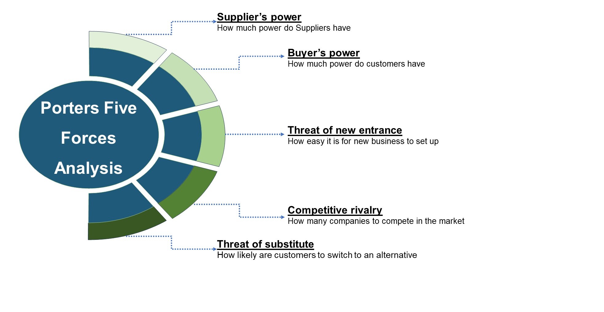
Porters Five Forces Analysis
We conduct Porter's Five Forces analysis to evaluate the competitive landscape of an industry, providing us with insights into factors that affect profitability and strategic positioning.
SWOT Analysis

Forecasting
We utilize a forecasting model to predict future consumption by considering parameters like population, economics, regulations, market competition, drivers, constraints, technology, and pricing. We also employ statistical techniques such as multilinear regression, exponential smoothing, moving average, ARIMA, and Monte Carlo simulations for accurate predictions. In econometric forecasting, we analyzed short-term and long-term event impacts, attributing values based on regulatory frameworks, economic factors, and market events.





 Speak to Our Analyst