Ayar Labs Tops $650M in Funding as NVIDIA Ships Silicon Photonics Switches
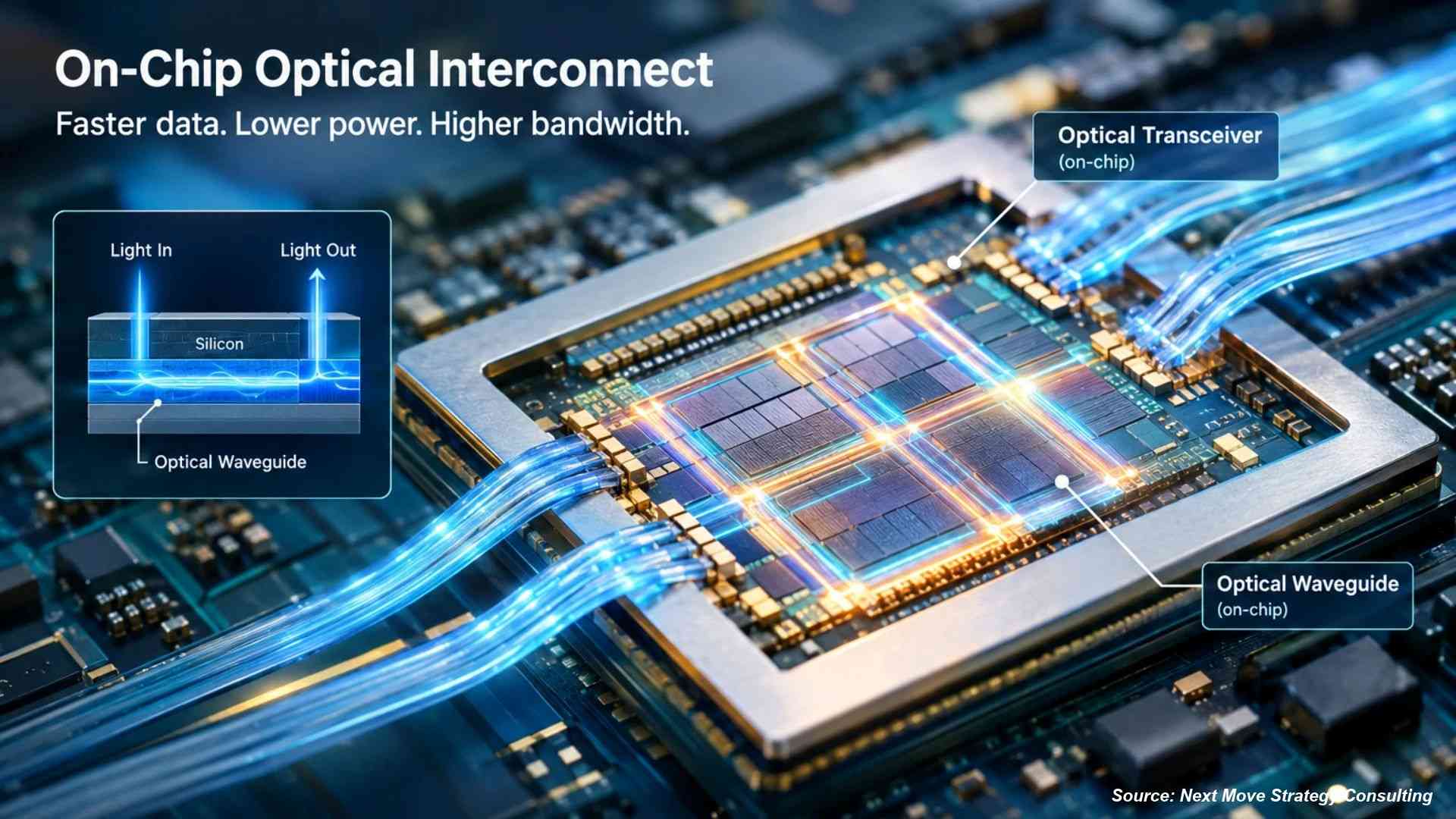
Ayar Labs Crosses $650 Million in Funding as NVIDIA Ships Silicon Photonics Switches and Industry Coalitions Rewrite the Rules of AI Interconnect Architecture
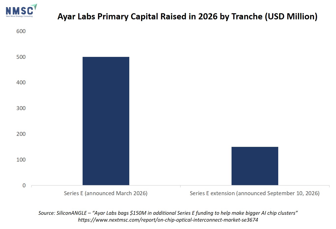
Ayar Labs Inc., the co-packaged optics (CPO) company backed by AMD, Intel, MediaTek, NVIDIA, and Wiwynn, announced on September 10, 2026, that it had extended its Series E round by an additional USD 150 million, bringing its total primary capital raised in 2026 alone to USD 650 million and its cumulative outside funding to just over USD 1 billion. The announcement — confirmed through the company's official press release and reported by SiliconAngle — arrived as NVIDIA simultaneously ramped its Spectrum-X Ethernet Photonics switch to full production, a co-packaged optics platform delivering up to 409.6 terabits per second of bandwidth with 5x better power efficiency than pluggable transceivers, with CoreWeave, Lambda, Meta, Microsoft, and Oracle Cloud Infrastructure named as first adopters.
These developments are unfolding against a market that is expanding at a pace few semiconductor segments can match. According to Next Move Strategy Consulting's On-Chip Optical Interconnect Market report, the global on-chip optical interconnect market was valued at USD 284.2 million in 2025 and is projected to reach USD 771.4 million by 2030, growing at a CAGR of 22.1% over the 2025–2030 forecast period. NMSC's proprietary research and analysis identifies AI-centric SoC design, the physical limits of copper SerDes at nanometre-scale geometries, and the commercial maturation of silicon photonics as the three structural forces compressing what was once a decade-long technology transition into a three-to-four-year commercialization sprint.
For More Information: Download FREE Sample on On-Chip Optical Interconnect Market Report
The Copper Bottleneck That Is Reshaping Semiconductor Architecture
The urgency behind the capital flows and product launches of 2026 traces directly to a measurable engineering constraint: copper electrical interconnects degrade in signal integrity, consume disproportionate power, and overheat when linking thousands of GPUs across multi-rack AI clusters. Ayar Labs CEO and co-founder Mark Wade stated in the company's September 10, 2026, funding announcement: "Copper interconnect is becoming the limiting factor for AI scale-up. This funding allows us to move faster on manufacturing-ready co-packaged optics at scale. We're deepening our work across the foundry and packaging ecosystem and growing our engineering capacity to support customer programs worldwide."
The company's TeraPHY optical engine chiplet — which integrates silicon photonics directly into the ASIC socket alongside the GPU — is designed to replace copper I/O with optical links that carry greater bandwidth at lower latency and a fraction of the energy cost. Ayar Labs' own product documentation states that TeraPHY delivers 5x to 10x more bandwidth, 10x lower latency, and 4x to 8x less power compared to electrical interconnects.
The new USD 150 million tranche will fund the company's transition to high-volume manufacturing, including the opening of a new Bengaluru Design Center in India. Sankara Venkateswaran, Vice President of Silicon Engineering at Ayar Labs, stated: "Our new Bengaluru Design Center supports our transition from technology development to commercialization and production. As customer demand and the complexity of our product roadmap increase, expanding our global engineering capacity will help us execute faster, support multiple development programs, and collaborate more closely with partners and customers across the region."
Wiwynn Corporation, a cloud IT and infrastructure provider for data centers, made a strategic investment in Ayar Labs earlier in 2026. William Lin, President and CEO of Wiwynn, stated: "Co-packaged optics is a foundational technology for the next generation of AI and cloud data centers. Through our collaboration and investment with Ayar Labs, we see a clear path to new architectures that reduce the power and complexity limits of copper interconnects, powering rack-scale deployment for the next wave of hyperscale AI data centers."
Wade told Reuters that the company aims to bring its technology to the mass market by early 2028, with all products qualified for volume production by end of 2027 to support customer ramp cycles in the 2028–2029 timeframe.
OFC 2026: An Industry Coalesces Around Optical Standards
The Optical Fiber Communication Conference (OFC 2026), held in Los Angeles in March 2026, produced a cluster of announcements that collectively signal the on-chip optical interconnect market's transition from prototype demonstrations to ecosystem-level standardization.
The most structurally significant development was the formation of the 400G Optical MSA (400 Gbps Optical Multi-Source Agreement) on March 23, 2026, by founding members Broadcom, Cisco, MACOM, NVIDIA, and Semtech. The MSA is tasked with developing specifications for optical interfaces that enable interoperable 400G optical solutions across transceivers and form factors produced by different manufacturers — a prerequisite for broad commercial deployment of co-packaged optics in hyperscale AI data centers.
Additional OFC 2026 developments of note included:
-
Tower Semiconductor and Oriole Networks announced a collaboration to commercialize nanosecond optical circuit switching for AI architectures, combining Oriole's PRISM Ultra networking platform — which claims 51.2 Tbps per xPU, 180-nanosecond xPU-to-xPU latency, and contention-free connectivity extending to one million nodes — with Tower's silicon photonics manufacturing platform.
-
NewPhotonics introduced its Syncra micro-ring modulator (MRM), a silicon photonics-based device that modulates PAM4 RF signals and maintains thermal stability without heaters or monitoring photodiodes — eliminating thermal crosstalk and addressing one of the most persistent yield challenges in high-density AI interconnect scaling.
-
ams OSRAM advanced a prototype micro-LED array for AI optical interconnects to the product-development phase, demonstrating a cut-off frequency exceeding 1 GHz and energy consumption below 2 pJ/bit — a performance level that, if sustained in production, would place the device within the ultra-low power budget tier that NMSC's proprietary research identifies as the critical threshold for embedded AI and edge inference applications.
-
POET Technologies established a strategic collaboration with LITEON to co-develop next-generation optical communication modules built on POET's patented optical interposer technology, with high-volume production targeted for 2027.
-
NLM Photonics began sampling its 1.6T and 3.2T photonic integrated circuits (PICs) fabricated on the GlobalFoundries AMF GP Process, and separately completed initial processing of silicon organic hybrid (SOH) modulators on Tower Semiconductor's PH18M silicon photonics platform.
-
Beeplux Semiconductor demonstrated a silicon photonics transmitter reaching 224 Gbps per lane, evaluated using a MACOM linear driver, with a combined electro-optical bandwidth exceeding 60 GHz — meeting the performance requirements for emerging 200G-per-lane optical links.
|
Company / Consortium |
Announcement |
Date |
Strategic Significance |
|
Broadcom, Cisco, MACOM, NVIDIA, Semtech |
Formation of 400G Optical MSA |
March 23, 2026 |
Establishes interoperability specifications for 400G optical interfaces across manufacturers |
|
Ayar Labs (+ AMD, Intel, MediaTek, NVIDIA, Wiwynn) |
Series E extended to USD 650M total |
September 10, 2026 |
Largest CPO-focused funding round to date; signals hyperscaler-backed manufacturing readiness |
|
Volantis |
USD 88M Series A for VCSEL-based photonic interconnect |
October 1, 2026 |
Targets AI memory wall via optical compute-to-memory links; CTO formerly led Micron's HBM program |
|
NVIDIA |
Spectrum-X Ethernet Photonics ramps to full production |
H2 2026 |
409.6 Tb/s bandwidth, 5x power efficiency; first adopters include Meta, Microsoft, Oracle |
|
Tower Semiconductor + Oriole Networks |
Silicon photonics collaboration for nanosecond OCS |
March 2026 |
Commercializes optical circuit switching for scale-up and scale-out AI architectures |
|
POET Technologies + LITEON |
Co-development of next-gen optical modules on optical interposer |
March 2026 |
High-volume production targeted for 2027 |
|
NewPhotonics |
Syncra heaterless micro-ring modulator (MRM) |
March 2026 |
Eliminates thermal crosstalk in high-density AI interconnect; addresses key yield barrier |
|
ams OSRAM |
Micro-LED array prototype: <2 pJ/bit, >1 GHz cut-off |
March 2026 |
Advances to product-development phase; targets ultra-low power AI optical I/O |
Volantis: A New Entrant Targets the AI Memory Wall
On October 1, 2026, Silicon Valley startup Volantis announced a USD 88 million Series A round co-led by Lachy Groom and Abstract Ventures, with named participants including John Doerr, VXI Capital, Triatomic, and Susa Ventures, bringing the company's total disclosed funding to USD 97 million since its founding in 2022.
Volantis is developing VCSEL-based photonic interconnects designed to link AI processors with memory pools over distances that copper electrical links cannot sustain without signal degradation. The company's stated engineering thesis — published in its PR Newswire funding announcement — is that optical waveguides can travel 200 mm or more, breaking the physical shoreline limit of HBM-based systems and enabling the aggregation of far greater memory capacity around a single processor than conventional electrical packaging allows.
The company's founding team carries direct pedigree in the problem it is attempting to solve. CEO Tapa Ghosh is a Thiel Fellow and former Y Combinator founder holding four patents. CTO Roy Meade previously led Micron's HBM program before serving as a Vice President at Ayar Labs. Director of Packaging Inderjit Singh is credited with helping build the industry's first CoWoS product — the advanced packaging platform TSMC now deploys for nearly every high-end AI accelerator.
Volantis has not yet published independently verified figures for achieved optical bandwidth, energy per bit, or production yield. Its first inference engines are targeted for 2027, though the company has not confirmed this as a committed roadmap date. The round nonetheless reflects a broader investor thesis that memory bandwidth — not raw compute — will be the defining constraint on AI progress through the end of the decade.
NMSC Strategic Perspective: What the Capital Concentration Signals for Market Structure
The on-chip optical interconnect market is undergoing a structural inflection that NMSC's proprietary research and analysis identifies as qualitatively different from prior photonics adoption cycles. Three dynamics are converging simultaneously in a way that compresses the typical technology-to-commercialization timeline.
-
First, the demand signal is no longer speculative. NVIDIA's Spectrum-X Ethernet Photonics switch — with 409.6 Tb/s bandwidth and 5x power efficiency over pluggable transceivers — is in full production with named hyperscaler customers. The formation of the 400G Optical MSA by Broadcom, Cisco, MACOM, NVIDIA, and Semtech in March 2026 establishes the interoperability framework that historically precedes broad ecosystem adoption. These are not research demonstrations; they are production commitments from the companies that set the purchasing agenda for global AI infrastructure.
-
Second, the capital concentration is self-reinforcing. Ayar Labs' USD 650 million in 2026 funding — backed by the same chipmakers whose products will integrate TeraPHY — creates a manufacturing readiness flywheel: foundry and packaging partners invest in process qualification because the customer base is credible; the customer base deepens because the supply chain is maturing. Volantis's USD 88 million Series A, arriving just three weeks after Ayar Labs' extension, confirms that investor appetite for optical interconnect bets extends beyond the established leaders to early-stage entrants targeting adjacent problems such as the AI memory wall.
-
Third, the segmentation of the competitive landscape is clarifying. NMSC's analysis identifies three distinct competitive tiers now forming: (1) hyperscaler-integrated CPO platforms (NVIDIA's Spectrum-X, Ayar Labs' TeraPHY); (2) photonic platform specialists targeting specific integration architectures (POET Technologies on optical interposers, Oriole Networks on optical circuit switching, NewPhotonics on heaterless MRMs); and (3) early-stage compute-to-memory optical startups (Volantis, Celestial AI — now part of Marvell following its December 2025 acquisition). Each tier competes for a different portion of the USD 771.4 million addressable market that NMSC projects by 2030, and the boundaries between tiers are likely to blur as co-packaged optics standards mature and chiplet interoperability frameworks such as UCIe 2.0 gain adoption.
The critical near-term risk NMSC's research identifies is manufacturing yield. Precision alignment of photonic components, wafer-level yield variability, and the thermal sensitivity of microring resonators remain the primary barriers between laboratory performance and volume production economics. Companies that resolve these yield challenges — through CMOS-compatible monolithic integration, heterogeneous packaging, or EPDA tool maturation — will capture disproportionate share of the market's growth between now and 2030.
Market Segmentation: Where the Growth Is Concentrated
By End-Use Application
SoCs for HPC/AI dominate on-chip optical interconnect adoption, accounting for 40.2% of usage intensity, according to NMSC's proprietary research and analysis. AI/ML accelerators represent the second-largest segment at 24.7%, followed by Network-on-Chip (NoC) at 15.1%, memory interfaces at 10.3%, and other embedded applications at 9.7%.
The concentration in HPC/AI SoCs reflects a specific engineering reality: deep neural network accelerators face data-movement bottlenecks that optical network-on-chip architectures can address with up to 6x improvement in energy-delay-area metrics compared to electrical interconnects, according to a 2024 review cited in NMSC's analysis.
By Photonic Platform
Silicon Photonics (SiPh) dominates the current on-chip optics landscape, benefiting from CMOS compatibility that enables integration with existing logic fabs and rapid deployment in AI accelerators and data centers. Lithium Niobate on Insulator (LNOI) is the fastest-growing platform, driven by its ultra-low loss and high-speed modulation characteristics that make it particularly suited to high-precision modulators and low-latency neuromorphic interconnects. Indium Phosphide (InP) retains a strong position in telecom-grade optical links and longer-wavelength applications where superior electro-optic performance is required.
By Integration Architecture
Heterogeneous integration — where photonic and electronic dies are fabricated separately and assembled — has emerged as the leading near-term approach, offering design flexibility, modular upgrades, and compatibility with existing packaging infrastructure. Monolithic integration is gaining traction in AI-centric SoCs for its compact footprint and low interconnect latency. 3D-stacked photonics, while still in early-stage development, has demonstrated 5.3 Tb/s bandwidth per mm² and energy efficiency of 120 fJ/bit in research settings, pointing to its potential as the dominant architecture for next-generation chiplet-based HPC packaging.
Regional Outlook
North America leads the global on-chip optical interconnect market, driven by the concentration of hyperscale data center investment, U.S. government support for domestic semiconductor manufacturing under the CHIPS Act, and the presence of the market's most active commercial players — including Ayar Labs, NVIDIA, Intel, and a growing cohort of silicon photonics startups. The U.S. dominates the regional picture, with defense electronics demand and AI infrastructure build-out reinforcing each other as demand drivers.
Asia-Pacific is the fastest-growing region, with China, Japan, South Korea, and India all scaling photonics R&D and manufacturing investment. South Korea's Samsung and SK Hynix are investing in optical interconnects for next-generation memory interfaces and AI chips. Japan's NTT and Fujitsu are advancing photonic packaging and chiplet integration. Ayar Labs' new Bengaluru Design Center — announced as part of its September 2026 funding extension — marks a concrete step toward India's integration into the global CPO supply chain.
Europe is advancing through the European Chips Act and Horizon Europe funding, with Germany's Fraunhofer Heinrich Hertz Institute and France's CEA-Leti anchoring regional R&D. The Fraunhofer HHI and 1Finity (a Fujitsu company) launched a long-term cooperation in March 2026 to advance open and disaggregated optical networks, including the joint SHINKA project funded by the German Federal Ministry of Research, Technology and Space and Japan's Ministry of Internal Affairs and Communications.
Competitive Landscape
The on-chip optical interconnect competitive landscape in 2026 is defined by three concurrent dynamics: hyperscaler-backed CPO platforms reaching production readiness, strategic acquisitions consolidating photonic IP, and a new wave of early-stage startups targeting the AI memory wall specifically.
Marvell's December 2025 acquisition of Celestial AI — which had raised over USD 330 million and achieved unicorn status on the strength of hyperscaler design-in commitments for its Photonic Fabric optical chiplets — represents the most significant consolidation event in the market's recent history, according to Cignal AI's optical component startup tracker.
AMD's May 2025 acquisition of EnoSemi, a Silicon Valley photonic integrated circuit IP specialist, accelerated AMD's entry into silicon photonics and positioned it to compete with NVIDIA's CPO advances in co-packaged optics and integrated communication.
iPronics, the Spanish silicon photonics startup developing optical circuit switches, expanded its global manufacturing capabilities in March 2026 through a deepened partnership with Fabrinet, establishing a dedicated manufacturing line for packaging, assembly, testing, and qualification of its ONE Series silicon photonic optical circuit switch, with volume production expected from the second quarter of 2026.
Key players tracked by NMSC's proprietary research include: Ayar Labs, OpenLight Photonics, Ranovus, Effect Photonics, Alcyon Photonics, POET Technologies, Polariton, iPronics, Intel Corporation, Celestial AI (now part of Marvell), Rockley Photonics, Avicena, PhotonICs Corporation, Oriole Networks, and Pilot Photonics.
Bottom Line
The on-chip optical interconnect market is no longer a technology roadmap item — it is an active capital deployment and product commercialization race. Ayar Labs' USD 650 million in 2026 funding, backed by AMD, Intel, MediaTek, NVIDIA, and Wiwynn, establishes co-packaged optics as a manufacturing-priority technology with a credible 2027–2028 volume production timeline. NVIDIA's Spectrum-X Ethernet Photonics switch, now in full production with five named hyperscaler customers, demonstrates that silicon photonics-based CPO can deliver 5x power efficiency gains at 409.6 Tb/s scale. The formation of the 400G Optical MSA by Broadcom, Cisco, MACOM, NVIDIA, and Semtech at OFC 2026 provides the interoperability framework that broad ecosystem adoption requires. Volantis's USD 88 million Series A, targeting the AI memory wall through VCSEL-based photonic interconnects, signals that investor conviction is extending beyond chip-to-chip links to compute-to-memory optical architectures. According to NMSC's proprietary research and analysis, the global on-chip optical interconnect market is projected to grow from USD 284.2 million in 2025 to USD 771.4 million by 2030 at a 22.1% CAGR — a trajectory that the events of 2026 are actively accelerating, not merely confirming.
About Next Move Strategy Consulting
Next Move Strategy Consulting is a premier market research and management consulting firm that has been committed to provide strategically analysed well documented latest research reports to its clients. The research industry is flooded with many firms to choose from, what makes NMSC different from the rest is its top-quality research and the obsession of turning data into knowledge by dissecting every bit of it and providing fact-based research recommendation that is supported by information collected from over 500 million websites, paid databases, industry journals and one on one consultations with industry experts across a diverse range of industry sectors. The high-quality customized research reports with actionable insights and excellent end-to-end customer service help our clients to take critical business decisions that enables them to move beyond time and have competitive edge in the industry.
We have been servicing over 1000 customers globally that includes 90% of the Fortune 500 companies over a decade. Our analysts are constantly tracking various high growth markets and identifying hidden opportunities in each sector or the industry. We provide one of the industry's best quality syndicate as well as custom research reports across 10 different industry verticals. We are committed to deliver high quality research solutions in accordance to your business needs. Our industry standard delivery solutions that ranges from the pre consultation to after-sales services, provide an excellent client experience and ensure right strategic decision making for businesses.
For more information, please contact:
Next Move Strategy Consulting
5th Floor 867 Boylston St, STE 500,
Boston, MA 02116, U.S.
E-Mail: [email protected]
Direct: +1-217-650-7991
Website: www.nextmsc.com
About the Author
 Sanyukta Deb
— Sanyukta Deb is Digital Marketing Team Lead at Next Move Strategy Consulting, where she has led content strategy and technical SEO for the firm's B2B market research publications for over 2 years. Her editorial process translates NextMSC's primary and secondary research — spanning technology, industrial, and consumer sectors — into commercial narratives, backed by search-intent, keyword, and competitive analysis. She brings 5 years of overall experience in digital marketing and content strategy.
Sanyukta Deb
— Sanyukta Deb is Digital Marketing Team Lead at Next Move Strategy Consulting, where she has led content strategy and technical SEO for the firm's B2B market research publications for over 2 years. Her editorial process translates NextMSC's primary and secondary research — spanning technology, industrial, and consumer sectors — into commercial narratives, backed by search-intent, keyword, and competitive analysis. She brings 5 years of overall experience in digital marketing and content strategy.
About the Reviewer
 Debashree Dey
— Debashree Dey is Assistant Manager at Next Move Strategy Consulting, where she supports cross-vertical market content and communications across diverse industries for 6 years. Her professional background includes senior content writing, communications, and published manuscript authorship, with experience developing audience-focused business narratives and maintaining clear, consistent messaging. Her role supports research-led content development and editorial quality across NextMSC publications.
Debashree Dey
— Debashree Dey is Assistant Manager at Next Move Strategy Consulting, where she supports cross-vertical market content and communications across diverse industries for 6 years. Her professional background includes senior content writing, communications, and published manuscript authorship, with experience developing audience-focused business narratives and maintaining clear, consistent messaging. Her role supports research-led content development and editorial quality across NextMSC publications.

















Add Comment