On-Chip Optical Interconnect Market By Integration Architecture (Monolithic, Heterogeneous, and 3D-Stacked Photonics), By Photonic Platform (SiPh, InP, LNOI and Others), By Modulation Scheme (Direct-Detect, and Coherent), By Performance Tier (Standard, Mid and High), By Link Distance (Intra-Die and Inter-Die), By End-Use Application (SoCs for HPC/AI, Network-on-Chip, Memory Interfaces and Others) – Global On-Chip Optical Interconnect Analysis & Forecast, 2025–2030
Industry Outlook
The On-Chip Optical Interconnect Market size was valued at USD 232.8 Million in 2024, and is expected to be valued at USD 284.2 million by the end of 2025. The industry is projected to grow, hitting USD 771.4 million by 2030, with a CAGR of 22.1% between 2025 and 2030.
The on-chip optical interconnect market is gaining momentum as data-intensive applications such as artificial intelligence, machine learning, and real-time analytics place unprecedented demands on processing speed and energy efficiency. Traditional electrical interconnects are increasingly challenged by signal integrity issues, bandwidth bottlenecks, and excessive power consumption, especially at nanometre-scale geometries. On-chip optical solutions offer a compelling alternative by enabling ultra-fast, low-latency communication between cores, memory blocks, and accelerators within a single chip. This has led to growing adoption in advanced processor architectures, particularly in AI accelerators and neuromorphic chips, where performance and efficiency are critical.
The market is being shaped by technological advancements in silicon photonics, photonic crystal waveguides, mirroring modulators, and monolithic integration techniques compatible with standard CMOS processes. These innovations are enabling higher data throughput, improved scalability, and reduced thermal overhead. Additionally, regulatory and industry-driven focus on energy-efficient design and sustainable computing is encouraging the development of optical interconnect standards for on-chip communication. As a result, chipmakers, research institutes, and fabless semiconductor firms are increasingly investing in R&D and IP development around on-chip optics to future-proof next-generation computing systems.
What are the Key On-Chip Optical Interconnect Industry Trends?
How Is Co-Packaged Optics Reshaping On Chip Optical Interconnect Market Growth?
With co-packaged optics (CPO) now predicted to become mainstream in hyperscale switches by 2025 (enabling 800G+ ports), the move to integrate optical engines directly with ASICs is accelerating. By reducing electrical link losses and slashing power per bit, CPO meets the ultra dense, high speed demands of AI inference systems. For semiconductor firms, this means aligning packaging roadmaps to CPO standards, collaborating with OIF/OCP, and prioritizing thermal design for optics in ASIC. Companies that develop modular, scalable CPO solutions now can build relationships with hyperscalers and claim first mover advantages as the technology transitions from lab to large scale deployment.
What Role Does Heterogeneous Integration and Multi Dimensional Multiplexing Play in Advancing On Chip Optical Interconnects?
An emerging breakthrough published in October 2024 demonstrated on chip optical links reaching multi tens Tb/s by using multi mode metamaterials across five modes and 88 wavelengths, delivering 38.2 Tb/s on a single chip and pointing to sub petabit/s potential. This trend shows how combining wavelength and mode division multiplexing with metamaterial waveguides can solve scaling limits imposed by electronics. Chipmakers should invest in R&D for digital metamaterials and partner with foundries to pilot multi mode interconnects, preparing architecture support for future Integrated Photonic Electronic SoCs capable of next level bandwidth.
How are Advanced Modulators and Hybrid Plasmonics Unlocking Ultra Fast On Chip Links?
Recent academic work demonstrates silicon modulators using slow light coupled resonator waveguides achieving over 110 GHz electro optic bandwidth and data rates beyond 110 Gb/s in ultra compact layouts. Alongside this, hybrid plasmonic waveguides offer nanoscale confinement with plasmonic dielectric synergy, pointing to future chip scale optical pathways that are both high speed and energy efficient. Foundries and design house teams should explore co design of hybrid plasmonic modulators within EPDA toolchains and prototype “slow light” modulators in advanced nodes, gaining differentiation through superior latency/power performance.
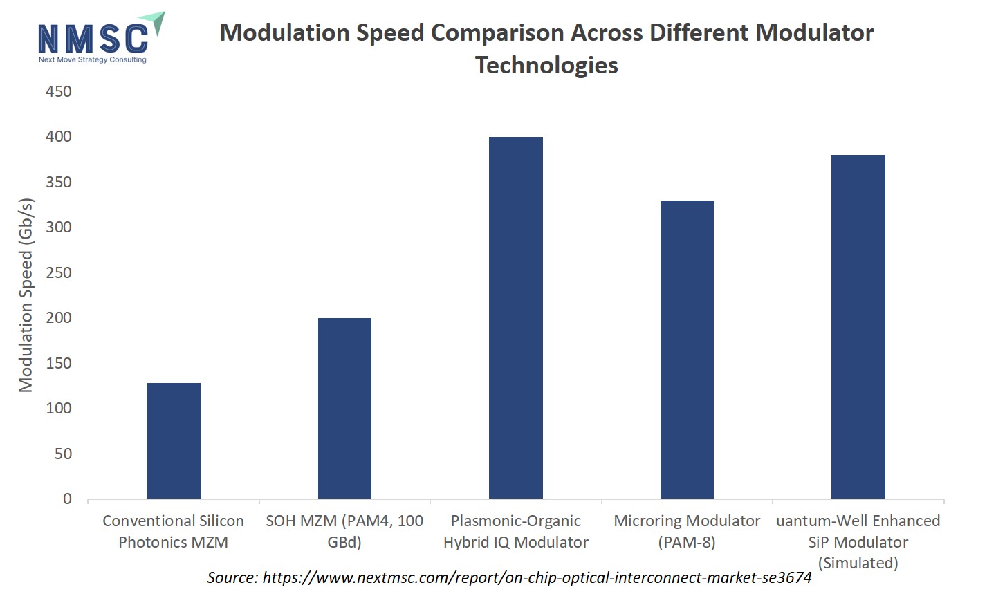
The infographic above illustrates a modulation speed comparison across different on-chip optical modulator technologies, highlighting the rapid advancements driving ultra-fast optical interconnects. Conventional silicon photonics Mach–Zehnder modulators (MZM) show baseline speeds around 125 Gb/s, while silicon–organic hybrid (SOH) MZMs operating at 100 GBd with PAM4 signaling push this to 200 Gb/s. More advanced approaches, such as plasmonic–organic hybrid IQ modulators, significantly increase performance, achieving speeds of 400 Gb/s within a compact footprint and with ultra-low energy consumption. Microring modulators employing PAM-8 reach 330 Gb/s, showcasing the potential of resonator-based designs for high-speed data transmission. Simulated results for quantum-well enhanced silicon photonics modulators further project speeds exceeding 380 Gb/s, pointing toward future scalability. Overall, the chart underscores how advanced modulators and hybrid plasmonics are unlocking unprecedented bandwidths, positioning them as critical enablers for next-generation on-chip optical links
Why is Standardization and EPDA Tool Support Critical for Commercialization?
Open standards like UCIe 2.0 (August 2024) bring interoperability to chiplet based optical integration, vital for broader ecosystem adoption. Meanwhile, Electronic Photonic Design Automation (EPDA) tools are closing the design-to-silicon gap for integrated PICs. As ecosystems coalesce around open RDVs and design stacks, companies that invest now in EPDA workflows and contribute to standard bodies will be best positioned to release robust, interoperable optical SoCs when market timing aligns.
What Are the Key Market Drivers, Breakthroughs, And Investment Opportunities That Will Shape the On-Chip Optical Interconnect Industry in Next Decade?
The on-chip optical interconnect market is rapidly evolving as the semiconductor industry seeks faster, energy-efficient alternatives to electrical interconnects for AI, high-performance computing, and advanced SoCs. Optical interconnects offer ultra-low latency, higher bandwidth density, and reduced thermal load—key advantages for data-intensive and real-time applications. As Moore’s Law slows, demand for scalable and efficient on-chip communication is driving innovation across photonic integration, waveguide miniaturization, and electro-optical modulation.
Breakthroughs in silicon photonics, photonic-electronic co-design, and multi-wavelength integration are paving the way for commercial adoption, particularly in AI accelerators and neuromorphic computing chips. Yet, the on-chip optical interconnect market must overcome fabrication complexity, yield challenges, and design-tool limitations. Regulatory trends pushing for greener data processing and increased chip-level performance also shape the strategic landscape. The next wave of investment will likely prioritize standardization, interoperability, and scalable photonic IP libraries.
Growth Drivers:
What’s Fueling the Rising Demand For Photonic Interconnects In AI Chips?
With AI workloads doubling every 3–4 months, electrical interconnects are becoming bottlenecks in neural network accelerators. On-chip optical links reduce power per bit while supporting massive parallel data movement, which is critical for transformer-based architectures. Companies targeting AI silicon must adopt photonic paths for intra-chip and near-chip data routing to maintain processing efficiency and edge inferencing speeds.
How Are Design Limitations In Electrical I/O Driving A Shift Toward Optics?
As chips become more heterogeneous and chiplets proliferate, electrical I/O struggles with bandwidth density and signal degradation. Optical interconnects eliminate crosstalk and minimize latency, enabling faster data movement in 2.5D/3D ICs. This shift creates urgency for semiconductor firms to integrate CMOS-compatible photonic components and co-design electro-optical layers in early architecture stages.
Growth Inhibitors:
What’s Hindering Large-Scale Adoption of On-Chip Optics?
Manufacturing complexity remains a major inhibitor. Precision alignment of photonic components, wafer-level yield variability, and thermal sensitivity of optical devices like microring resonators pose scale-up challenges. Without robust, cost-efficient integration techniques and mature EDA tools, commercial yields may fall short—slowing adoption in cost-sensitive markets.
Where Is the Next Major Investment Opportunity in the On-Chip Optical Interconnect Market?
Electronic-Photonic Design Automation (EPDA) tools present a critical investment frontier. As demand grows for rapid prototyping and custom photonic circuit integration, startups and EDA vendors that offer intuitive, foundry-compatible tools will attract strong interest. Supporting open standards and chiplet interoperability within these tools could unlock design scalability and market entry for a broader range of players.
How On-Chip Optical Interconnect Market Is Segmented in This Report, And What Are the Key Insights from the Segmentation Analysis?
By Integration Architecture Insights
How Are Monolithic, Heterogeneous, and 3D-Stacked Architectures Shaping the On-Chip Optical Interconnect Market?
On the basis of Integration Architecture, the on-chip optical interconnect market report is segmented into Monolithic Integration, Heterogeneous Integration and 3D-Stacked Photonics.
Monolithic integration, where photonic and electronic components are fabricated on a single substrate—is gaining traction in AI-centric SoCs due to its compact footprint, low interconnect latency, and improved energy efficiency. Recent advances in silicon photonics and CMOS-compatible photonic integration have enabled seamless electro-optical co-design, reducing overhead caused by off-chip communication. According to industry reports, monolithic photonics can reduce power consumption and improve bandwidth density compared to hybrid approaches, particularly in data-intensive AI processors. While material compatibility and thermal management remain technical hurdles, companies that develop in-house photonic integration capabilities can differentiate through tighter vertical control, optimized yield, and performance tuning at the design and fabrication levels.
Heterogeneous integration, where photonic and electronic dies are fabricated separately and then assembled has become a leading approach for enabling scalable, high-performance on-chip optical systems. Its inherent design flexibility allows developers to pair optimized photonic components with advanced logic dies, supporting modular upgrades and quicker innovation cycles. This method also eases thermal management by physically separating heat-intensive and light-sensitive components. As industry roadmaps move toward chiplet-based systems and disaggregated architectures, heterogeneous integration aligns well with existing packaging infrastructure. For companies transitioning to optical interconnects, this architecture reduces the need for full-scale fabrication overhauls and shortens time to market, making it a practical and strategic entry point into photonic integration.
3D-stacked photonics, stacking photonic layers vertically atop logic or memory dies,has demonstrated impressive potential, with a dense 2023 study showing 5.3 Tb/s bandwidth per mm² and energy efficiency of 120 fJ/bit via dense 3D integration of photonic and electronic chips. While still in early-stage development, this architecture significantly reduces interconnect latency and energy costs compared to traditional approaches. Chip designers and foundries that invest in vertical optical coupling, hybrid bonding, and thermal-aware designs now will position themselves as leaders in next-gen chiplet-based and HPC packaging ecosystems.
By Photonic Platform Insights
How Are Silicon Photonics, InP, LNOI, and Polymer Platforms Shaping the on Chip Optical Interconnect Market?
Based on Photonic Platform, the on-chip optical interconnect market is segmented into Silicon Photonics (SiPh), Indium Phosphide (InP), Lithium Niobate on Insulator (LNOI) and Polymer / Other Emerging.
Silicon Photonics dominates the current on-chip optics landscape valued at approximately USD 2.88 billion in 2025 and growing at ~23–25% CAGR through 2030. Its advantage comes from CMOS compatibility, enabling integration with existing logic fabs and rapid deployment in AI accelerators and data centers. For chip vendors, adopting silicon photonics offers a practical path to scale bandwidth while minimizing cost and leveraging mature supply chains for fast time to market.
The global InP wafer market is expected to grow from about USD 205 million in 2024 to over USD 570 million by 2033 at a CAGR of ~12%. Known for its superior electro-optic performance in lasers and detectors, InP is ideal for telecom-grade optical links and longer wavelengths. Companies aiming for maximum optical efficiency and range, especially in sensing or inter-chip communications, should invest in hybrid integration strategies that blend silicon’s scalability with InP’s high-performance photonic elements.
LNOI is gaining traction for its ultra-low loss and high-speed modulation, with thin-film LNOI projected to hit nearly USD 1 billion by 2029, growing at nearly 98% CAGR. This platform suits high-precision modulators and low-latency neuromorphic interconnects. Companies focusing on cutting-edge modulators and optical sensors can capitalize on LNOI’s unique properties by partnering with pioneers in thin-film LN fabrication to integrate these modulators into next-gen photonic SoC designs
Polymer-based and other emerging photonic materials are carving out roles in flexible interconnects, bio-photonics, and sensor-rich environments. Though their market share is still modest compared to SiPh or InP, these platforms offer rapid prototyping and low-cost fabrication. Startups and equipment vendors can leverage polymers for specialized optical components (e.g., flexible waveguides) and collaborate with universities to mature these platforms into commercially viable, application-specific solutions.
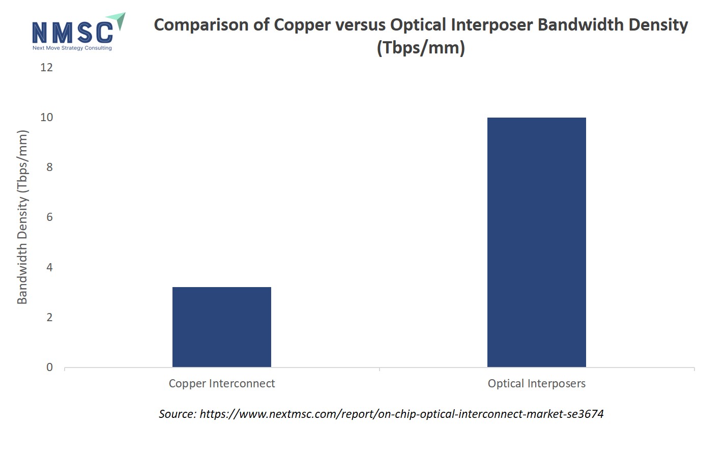
The above chart highlights the significant performance advantage of optical interposers over traditional copper interconnects in terms of bandwidth density. While copper interconnects provide around 3 Tbps/mm, optical interposers achieve approximately 10 Tbps/mm, more than three times higher. This stark contrast demonstrates why the industry is increasingly shifting towards optical interconnect solutions for on-chip communication. The growing demand for high-speed data transfer, driven by advanced computing, AI workloads, and data center requirements, makes optical interposers a more scalable and efficient alternative. Their ability to handle larger bandwidth while minimizing signal loss and power consumption positions them as a key enabler in the future growth of the on-chip optical interconnect market.
By Modulation Scheme Insights
How Do Direct Detect and Coherent Modulation Schemes Shape the On Chip Optical Interconnect Market?
Based on Modulation Scheme, the on-chip optical interconnect market is bifurcated into Direct-Detect (NRZ, PAM-4) and Coherent (QPSK, QAM-16+).
Direct detect modulation, especially PAM 4 is leading short reach on chip interconnect use with its simplicity and low power needs. Reddit discussions highlight deployment of 400 GbE PAM 4 optics inside data centers due to lower cost and energy compared to coherent links. With next gen 800 GbE PAM 4 optics leveraging 100 Gb/s per lane, this scheme remains the go to for cost and power sensitive applications. Companies should optimize PAM 4 implementation, pushing lane rates while ensuring robust signal integrity and minimal thermal impact.
Coherent schemes using QPSK and higher order QAM (e.g., 16 QAM) excel in long distance high bandwidth use cases. In 2023, 1.9 million coherent transceivers were shipped, with hyperscalers accounting for 38% of demand. Modules at 400 Gb/s and 800 Gb/s are growing rapidly, delivering up to 60% spectral efficiency gains with significantly reduced power footprints. For on chip optical interconnects requiring maximum data density, investing in coherent DSP development and compact, power efficient modulators can provide a competitive differentiation.
By Performance Tier Insights
How Do Capacity Tiers—Standard, Mid, and High—Define the On Chip Optical Interconnect Market?
On the basis of capacity, the on-chip optical interconnect market is segmented into Standard (<25 Gbps/lane), Mid (25–100 Gbps) and High (>100 Gbps).
Standard capacity links below 25 Gbps per lane remain essential in edge computing, IoT, and automotive domains. These segments favor simplicity, lower cost, and minimal power, rather than sheer speed. As 5G densification grows, low rate optical links offer reliable, low-latency connectivity between sensors and microcontrollers. Companies targeting these markets should focus on optimizing modulators and packaging for low thermal impact and rugged deployment environments—leveraging optical’s ground-up advantages over copper in space-constrained systems.
The 10–50 Gbps and 41–100 Gbps bands accounted for over 26% and a rising share of optical interconnect revenue in 2023, respectively. This mid-tier is ideal for enterprise and mid-scale cloud deployments, streamlining migration paths from legacy systems to modern fabrics without cost-prohibitive upgrades. Companies can capitalize by developing modular PAM 4 optical engines that balance performance and cost. Focusing on efficient forward-error correction and robust lane scalability will aid rapid adoption.
High-capacity optical links exceeding 100 Gbps per lane are becoming critical in supporting the explosive data demands of hyperscale AI, machine learning, and high-performance computing environments. These links enable ultra-fast, low-latency communication across chiplets and memory blocks, key for training large-scale models and real-time inferencing. As bandwidth demands continue to scale, the industry is shifting toward co-packaged optics and advanced modulation schemes to sustain performance while minimizing power consumption. Chipmakers prioritizing energy-efficient, high-density optical interconnects will be better positioned to serve next-generation compute architectures.
By Link Distance (µm-mm) Insights
How Are Intra Die (<1 mm) and Inter Die (1 mm–1 cm) Links Defining the On Chip Optical Interconnect Market?
On the basis of Link Distance (µm-mm), the on-chip optical interconnect market is segmented into Intra-Die (<1 mm) and Inter-Die (1 mm–1 cm).
Intra die optical links, spanning under 1 mm, are critical for enabling high-speed data transfers within a single chip. Research shows that on chip waveguides can transmit across densely packed components with minimal delay and energy overhead compared to traditional metal interconnects. This proximity enables chip designers to reduce latency in AI and signal-processing SoCs. For chipmakers, embedding short optical paths in the design phase and collaborating with fabrication partners ensures tight integration and better yield optimization.
Inter die optical links spanning millimeters to a centimeter are emerging as a powerful solution for high-density chiplet communication. A 2024 study demonstrated free standing polymer waveguides as long as 900 µm with controlled losses, opening pathways for die-to-die interconnects. Additionally, die-to-die optical chiplets bridge in-package I/O bandwidth gaps, enabling low power, high speed data transfer across separate modules. For system integrators and packaging vendors, adopting photonic chiplet standards and developing optical-aware substrates will accelerate integrated multi-die architectures.
By Power Budget Insights
How Are Ultra-Low, Moderate, and Standard Power Budgets Defining the On Chip Optical Interconnect Market?
On the basis of Power Budget, the on-chip optical interconnect market is segmented into Ultra-low (<1 pJ/bit), Moderate (1–10 pJ/bit) and Standard (>10 pJ/bit).
Ultra low power interconnects—delivering sub 1 pJ/bit efficiency are moving from theory to practice. A recent 2023 study demonstrated 120 fJ/bit links via 3D-integrated photonic-electronic chips, achieving impressive energy savings and 5.3 Tb/s/mm² bandwidth density. Such breakthroughs are vital for edge AI, wearable and implantable devices. Chipmakers should focus on 3D photonic integration, co-designed transmitters and receivers, and collaborations with foundries offering 3D photonics processes to embed ultra-efficient optical layers at scale.
Moderate-power links in the 1–10 pJ/bit range represent the current industry workhorse. Optical I/O chiplets, such as Ayar Labs’ TeraPHY, typically operate at <5 pJ/bit—the standard for today’s optical packages, enabling cost-effective, scalable deployment in HPC and data-centre SoCs. Designers aiming for broad adoption should optimize lane energy at ~3–8 pJ/bit, integrate WDM strategies, and ensure packaging supports thermal stability to hit these moderate-power targets efficiently.
Standard interconnects exceeding 10 pJ/bit are still prevalent in legacy systems and early-stage optical implementations. Silicon photonics links in telecom demonstrated ~16 pJ/bit in early zero-change CMOS chips, dominated by off-chip laser inefficiencies. For these segments, the priority is lowering link cost and simplifying integration. Companies servicing legacy markets should focus on hybrid photonic-electronic modules and incremental upgrades, introducing improved modulators and drivers to reduce energy below the >10 pJ/bit threshold without overhauling existing infrastructure.
By End-User Insights
How Are On Chip Optical Interconnects Serving Different End User Segments?
On the basis of end-user, the on-chip optical interconnect market is segmented SoCs for HPC/AI, Network-on-Chip (NoC), AI / ML Accelerators, Memory Interfaces and Other Embedded.
On-chip optical interconnects are gaining traction in HPC and AI SoCs to overcome bandwidth and energy challenges. A 2024 review highlights that DNN accelerators face significant data-movement bottlenecks, with optical NoCs potentially improving energy-delay-area metrics by up to 6× compared to electrical interconnects. Integrating optical pathways early in the SoC design flow empowers designers to alleviate bottlenecks in AI and accelerators, ensuring scalable performance for future compute-intensive workloads.
The NoC market is exploring optical integration to manage latencies and energy in mesh and hierarchical designs. Signature designs like FlooNoC demonstrate 0.15 pJ/B per hop at 645 Gbps using wide links. Optical NoCs can deliver high-speed, low-energy interconnect fabrics, drive smarter architectural choices and reduce thermal overhead.
AI/ML accelerators are increasingly constrained by internal bandwidth limits. Optical interconnects bypass electrical wiring constraints, enabling faster, low-latency data transfer between processing and memory tiles. For companies building domain-specific AI chips, integrating optical data lanes within accelerator blocks can boost performance-per-watt dramatically and support next-gen transformer and convolutional model workloads efficiently.
Memory interfaces are facing constraints as DRAM and emerging NVM push for higher speeds. Optical links can support multi-terabit/s interfaces with lower energy per bit, addressing thermal and signal-integrity challenges. Embedding short-span optical interfaces between controller and memory stacks offers a solution for future HBM or on-chip cache hierarchies, unlocking next-level throughput in data-heavy applications like real-time analytics.
Beyond mainstream domains, optical interconnects are finding niches in automotive, medical devices, and IoT embedded systems, where low power and EM immunity matter. Optical links offer robust performance in EMI-heavy or harsh environments. Developers in these segments can explore flexible waveguide integration or polymer optical paths to deliver optical communication advantages in compact, rugged embedded platforms.
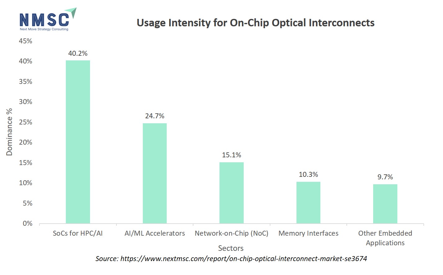
The above chart illustrates the usage intensity of on-chip optical interconnects across different semiconductor sectors. The bar chart shows that SoCs for HPC/AI dominate the usage with a 40.2% share, indicating that high-performance and AI-focused systems are the primary drivers of adoption. AI/ML accelerators follow with 24.7%, reflecting their growing demand for high-speed, low-latency interconnects. Network-on-Chip (NoC) solutions account for 15.1% of usage, while memory interfaces and other embedded applications each represent 10.3% and 9,7%, highlighting their relatively lower but still notable role in leveraging optical interconnect technologies. Overall, the chart conveys a clear hierarchy of sectoral adoption, emphasizing the concentration of usage in high-performance computing and AI domains.
Regional Outlook
The market is geographically studied across North America, South America, Europe, the Middle East & Africa, and Asia Pacific, and each region is further studied across countries.
On-Chip Optical Interconnect Market in North America
North America leads in the on-chip optical interconnect market due to robust investments in AI, HPC, and advanced semiconductor technologies. The presence of major tech firms, R&D institutions, and government support for domestic chip manufacturing boosts regional growth. Silicon photonics startups, such as Ayar Labs, and heavyweights like Intel and Nvidia, are accelerating commercialization of optical interconnects in cloud data centers and AI accelerators.
On-Chip Optical Interconnect Market in U.S.
The U.S. dominates the North American market, driven by strong semiconductor R&D funding, defense electronics demand, and hyperscale data center growth. Government initiatives like the CHIPS Act are fostering domestic manufacturing and innovation. Companies are focusing on photonic integration to reduce power consumption and increase bandwidth in AI, quantum computing, and 5G infrastructure, strengthening the country’s leadership in this domain.
On-Chip Optical Interconnect Market in Canada
Canada contributes moderately, with growth driven by academic research, photonics startups, and cross-border collaborations with U.S. tech giants. Universities and institutes like the University of Toronto and CMC Microsystems support photonics R&D. Government-backed innovation programs aim to commercialize lab-scale technologies into scalable photonic interconnects for quantum computing, AI chips, and smart manufacturing applications.
On-Chip Optical Interconnect Market in Europe
Europe is emerging as a strategic region in the on-chip optical interconnect landscape, fueled by initiatives like Horizon Europe and the European Chips Act. Germany, France, and the U.K. are at the forefront, pushing for semiconductor sovereignty. Investments in photonic integration, packaging, and heterogeneous integration are enabling European firms to play a growing role in AI and data center chip design.
On-Chip Optical Interconnect Market in U.K.
The U.K. focuses on integrated photonics through government-supported initiatives and partnerships with academic institutions like the University of Southampton. The country is investing in photonic systems for quantum computing and AI acceleration, offering opportunities for optical interconnect players. Startups are also exploring silicon-photonics-based solutions for defense and telecom applications.
On-Chip Optical Interconnect Market in Germany
Germany is a key player in Europe's chip ecosystem, with significant investment in silicon photonics and optoelectronics. Firms like Infineon and research centers such as Fraunhofer are exploring on-chip optical interconnects for automotive AI, industrial IoT, and high-speed computing. The government’s emphasis on digitalization and Industry 4.0 accelerates demand for high-bandwidth, low-latency communication within chips.
On-Chip Optical Interconnect Market in France
France’s on-chip optical interconnect market is supported by national strategies promoting photonics and semiconductor innovation. Institutions like CEA-Leti and collaborations with the European Union are driving R&D in integrated optics and chip-scale communications. Applications span from aerospace to telecommunications, creating a strong demand for energy-efficient, high-speed interconnect solutions.
On-Chip Optical Interconnect Market in Italy
Italy is gradually entering the photonics space, supported by EU funding and domestic digital transformation plans. Universities and startups are working on early-stage photonic ICs, with applications in defense electronics, AI hardware, and telecommunications. However, compared to France and Germany, Italy’s commercial adoption of on-chip optical interconnects remains in its infancy.
On-Chip Optical Interconnect Market in Spain
Spain is investing in photonics research through its national science strategy and EU-backed programs. Research centers like ICFO (Institute of Photonic Sciences) contribute to advancements in silicon photonics and optical interconnects. While commercial uptake is still limited, Spain’s academic prowess and growing semiconductor ambitions provide a foundation for future growth.
On-Chip Optical Interconnect Market in Nordics
The Nordic countries, particularly Sweden and Finland, are advancing in photonics research and chip-level optical innovations. Companies like Nokia are integrating photonics into telecom hardware, while universities explore applications in quantum and AI. Public-private partnerships and government-backed R&D are catalyzing the growth of on-chip optical technologies in this region.
On-Chip Optical Interconnect Market in Asia-Pacific
Asia-Pacific is expected to be the fastest-growing region, with massive investments from China, Japan, South Korea, and India. This region benefits from strong electronics manufacturing ecosystems, large-scale AI deployments, and 5G rollouts. Governments are supporting chip self-sufficiency and photonics R&D, which boosts demand for high-speed, low-power interconnects in SoCs.
On-Chip Optical Interconnect Market in China
China is rapidly scaling its photonic chip capabilities through heavy government support, especially under its "Made in China 2025" initiative. Companies like Huawei and HiSilicon are developing integrated optical solutions for AI chips, data centers, and telecom systems. The push for domestic chip production and reduced dependency on Western technology fuels significant investment in on-chip optical technologies.
On-Chip Optical Interconnect Market in Japan
Japan's advanced electronics industry is embracing silicon photonics and optical interconnects for HPC and 5G systems. Companies like NTT and Fujitsu are actively researching photonic packaging and chiplet integration. With strong governmental backing for semiconductor self-reliance and a culture of precision engineering, Japan is positioned to become a major hub for optical interconnect innovation.
On-Chip Optical Interconnect Market in India
India is gradually entering the on-chip optical interconnect space, driven by its booming electronics sector and government incentives like the Semiconductor Mission. While the ecosystem is still nascent, academic institutions and startups are beginning to explore silicon photonics. With a growing focus on AI and data center infrastructure, India presents long-term growth potential.
On-Chip Optical Interconnect Market in South Korea
South Korea, home to giants like Samsung and SK Hynix, is investing in optical interconnects for next-gen memory interfaces, AI chips, and mobile SoCs. Government-backed R&D and corporate initiatives aim to integrate photonic elements into chiplets to reduce latency and improve energy efficiency. Its semiconductor leadership positions it strongly in this space.
On-Chip Optical Interconnect Market in Indonesia
Indonesia's market is currently in the early development phase, with limited but growing interest in photonics and high-speed interconnects. Government initiatives to develop domestic chip capabilities and digital infrastructure may create future opportunities. Collaborations with ASEAN countries and tech firms could help accelerate adoption of on-chip optical interconnect technologies.
On-Chip Optical Interconnect Market in Australia
Australia’s involvement in the on-chip optical interconnect market is largely research-oriented, led by institutions like the University of Sydney and ANU. Government grants support projects in quantum photonics and chip-scale communication systems. Though the commercial sector is still emerging, Australia’s strong academic base lays a foundation for long-term growth.
On-Chip Optical Interconnect Market in Latin America
Latin America is still in the early adoption stage of on-chip optical interconnects, with minimal local manufacturing. However, increasing investments in AI infrastructure and cloud computing in countries like Brazil and Mexico may spur demand. Cross-border tech partnerships and government-backed digital initiatives could eventually foster growth in optical interconnect technologies.
On-Chip Optical Interconnect Market in Middle East and Africa
The Middle East & Africa region is at a nascent stage, with market activity concentrated in tech-driven economies like Israel and the UAE. Israel, in particular, shows promise due to its strong semiconductor R&D and photonics startups. Regional interest in AI, smart cities, and defense electronics could catalyze future demand for optical interconnects.
Competitive Landscape
Which Companies Dominate the On-chip Optical Interconnect Industry and How Do They Compete?
The on-chip optical interconnect market is witnessing rapid transformation, fueled by breakthroughs in silicon photonics, chiplet architectures, and AI-centric system design. As traditional electrical interconnects face limitations in speed, power, and density, leading companies are racing to integrate optical solutions directly onto chips to meet the growing demands of high-performance computing, data centres, and AI accelerators. This competitive landscape features a mix of established semiconductor giants and disruptive startups, each deploying unique strategies, from innovation-led product development to mergers and acquisitions, to capture market share and build end-to-end optical ecosystems. Understanding how these players operate, innovate, and collaborate offers key insights into the future trajectory of chip-scale optical communication.
Market Dominated by On-chip Optical Interconnect Giants and Specialists
The on-chip optical interconnect market is led by a mix of specialized startups and semiconductor giants. Key players include Ayar Labs, Lightmatter, Lightelligence, Broadcom, Nvidia, and Coherent Corp. Startups like Ayar Labs and Lightmatter are pioneering chip-to-chip optical links and photonic computing, while traditional players such as Nvidia and Broadcom are integrating optical interconnect IP into their high-performance SoCs and AI accelerators. The competition is intensifying across applications, ranging from data centers to AI and HPC workloads, where latency and bandwidth efficiency are critical. Each company is striving to carve out market share either by innovating around photonic chiplets or by embedding integrated optics into next-gen chip designs. This convergence of optical networking and compute is reshaping competitive dynamics across both silicon photonics and system-on-chip industries.
Innovation and Adaptability Drive Market Success
To stay ahead, leading players are embracing new packaging techniques like co-packaged optics (CPO), chiplet-based designs, and heterogeneous integration. Ayar Labs, for example, has developed TeraPHY, a chiplet offering ultra-low latency optical I/O integrated directly into CPUs and GPUs. Nvidia is experimenting with photonic interconnects to support its multi-die GPU architectures, especially for AI workloads. Lightelligence has unveiled optical AI accelerators using photonic circuits for matrix multiplication showing potential in both speed and energy savings. Lightelligence initially demonstrated its PACE (Photonic Arithmetic Computing Engine) platform—an integrated photonic–electronic chip stack designed for matrix multiplication and hard computational problems. It achieves hundreds of times faster performance and dramatically lower power consumption compared to conventional processors. These companies are also rapidly expanding through collaborations with foundries and hyperscalers. Innovation is no longer just about photonic performance but also system integration, power savings, and thermal management. Adaptability to shifting architectures—such as disaggregated compute and memory—has become a key differentiator in a market driven by AI and cloud computing.
Market Players to Opt for Merger & Acquisition Strategies to Expand their Presence
Strategic acquisitions are becoming crucial as companies look to scale quickly and integrate vertically. In 2024, Nokia acquired Infinera for USD 2.3 billion, adding advanced photonic integrated circuits (PICs) and coherent optics to its portfolio, bridging network optics with on-chip solutions. This acquisition integrates advanced photonic ICs and coherent optics into Nokia’s portfolio, allowing it to challenge peers like Ciena and Huawei, especially in North America and hyperscaler markets.
List of Key On-chip Optical Interconnect Companies
-
Openlight Photonics Inc.
-
Ranovus
-
Effectphotonics
-
Alcyon Photonics
-
POET Technologies Inc.
-
Polariton
-
Celestial AI.
-
Rockley Photonics
-
Avicena
-
Oriole Networks
-
Cisco investments
-
ASE Technology holding
-
Global Foundries
What Are The Latest Key Industry Developments?
-
June, 2024 – Intel’s Integrated Photonics Solutions group showcased its OCI chiplet co packaged with a CPU at OFC 2024. This demo delivered 64×32 Gbps optical I/O channels over 100 m fiber—boosting bandwidth, lowering power and enabling AI/data center scaling.
-
April, 2025 – Ayar Labs introduced its TeraPHY chiplet, offering 8 Tbps bandwidth using the UCIe standard. It combines silicon photonics with CMOS to reduce latency and power—making optical interconnects more modular and ecosystem-friendly.
-
March, 2025 – At GTC 2025, NVIDIA introduced its Spectrum X and Quantum X silicon photonics switch ASICs, achieving 3.5× lower power, reduced latency, and multi million GPU scalability—signaling a major leap for AI datacenter networks.
-
May, 2025 – AMD completed its acquisition of EnoSemi, a Silicon Valley PIC IP specialist. This move accelerates AMD’s entry into silicon photonics, empowering its AI and HPC chips to rival NVIDIA’s advances in co packaged optics and integrated communication.
-
February, 2025 – STMicroelectronics and Amazon Web Services revealed a co developed photonics data center transceiver chip, leveraging optical instead of electrical interconnects. Set for production in France later this year, it targets faster and more energy efficient AI infrastructure.
What Are The Key Factors Influencing Investment Analysis & Opportunities In On-Chip Optical Interconnect Market?
The sector has seen significant venture activity, especially in optical AI fabric startups. In March 2025, Celestial AI secured USD 250 M, raising its total to USD 515 M, targeting photonic compute-to-memory interconnects for AI systems. Earlier in Q4 2024, Lightmatter closed a USD 400 M Series D, valuing the company at USD 4.4 Billion; plus, Ayar Labs raised USD 155 M, pushing its valuation over USD 1 Billion. In Europe, case studies include PHOTON IP’s USD 5.27 Million seed in January 2025 and Black Semiconductor’s USD 296.5 Million Series A in June 2024, backed by Porsche Ventures and IPCEI funds. This influx underscores growing investor confidence, especially where chip-to-chip speed and energy efficiency meet AI demands, with hotspots in Silicon Valley and European deep-tech hubs, offering high-growth opportunities for fab-scale and integration-focused ventures.
Key Benefits for Stakeholders:
Next Move Strategy Consulting (NMSC) presents a comprehensive analysis of the on-chip optical interconnect market, covering historical trends from 2020 through 2024 and offering detailed forecasts through 2030. Our study examines the market at global, regional, and country levels, providing quantitative projections and insights into key growth drivers, challenges, and investment opportunities across all major on-chip optical interconnect segments.
The on-chip optical interconnect industry offers unique advantages for a wide range of stakeholders. Investors benefit from strong growth potential driven by AI, HPC, and cloud demand, with high ROI in companies advancing photonic integration and chiplet ecosystems. Policymakers gain strategic value through enhanced semiconductor sovereignty, energy-efficient infrastructure, and national security capabilities, aligning with green tech and digital economy goals. Meanwhile, customers, such as hyperscalers, AI startups, and system integrators—gain faster, low-latency, and scalable chip communication, improving performance while reducing energy and cooling costs. Collectively, the ecosystem supports innovation, job creation, and global competitiveness in next-generation computing architectures.
Report Scope:
|
Parameters |
Details |
|
Market Size in 2025 |
USD 284.2 million |
|
Revenue Forecast in 2030 |
USD 771.4 million |
|
Growth Rate |
CAGR of 22.1% from 2025 to 2030 |
|
Analysis Period |
2024–2030 |
|
Base Year Considered |
2024 |
|
Forecast Period |
2025–2030 |
|
Market Size Estimation |
Million (USD) |
|
Growth Factors |
|
|
Countries Covered |
28 |
|
Companies Profiled |
15 |
|
Market Share |
Available for 10 companies |
|
Customization Scope |
Free customization (equivalent up to 80 analyst-working hours) after purchase. Addition or alteration to country, regional & segment scope. |
|
Pricing and Purchase Options |
Avail customized purchase options to meet your exact research needs. |
|
Approach |
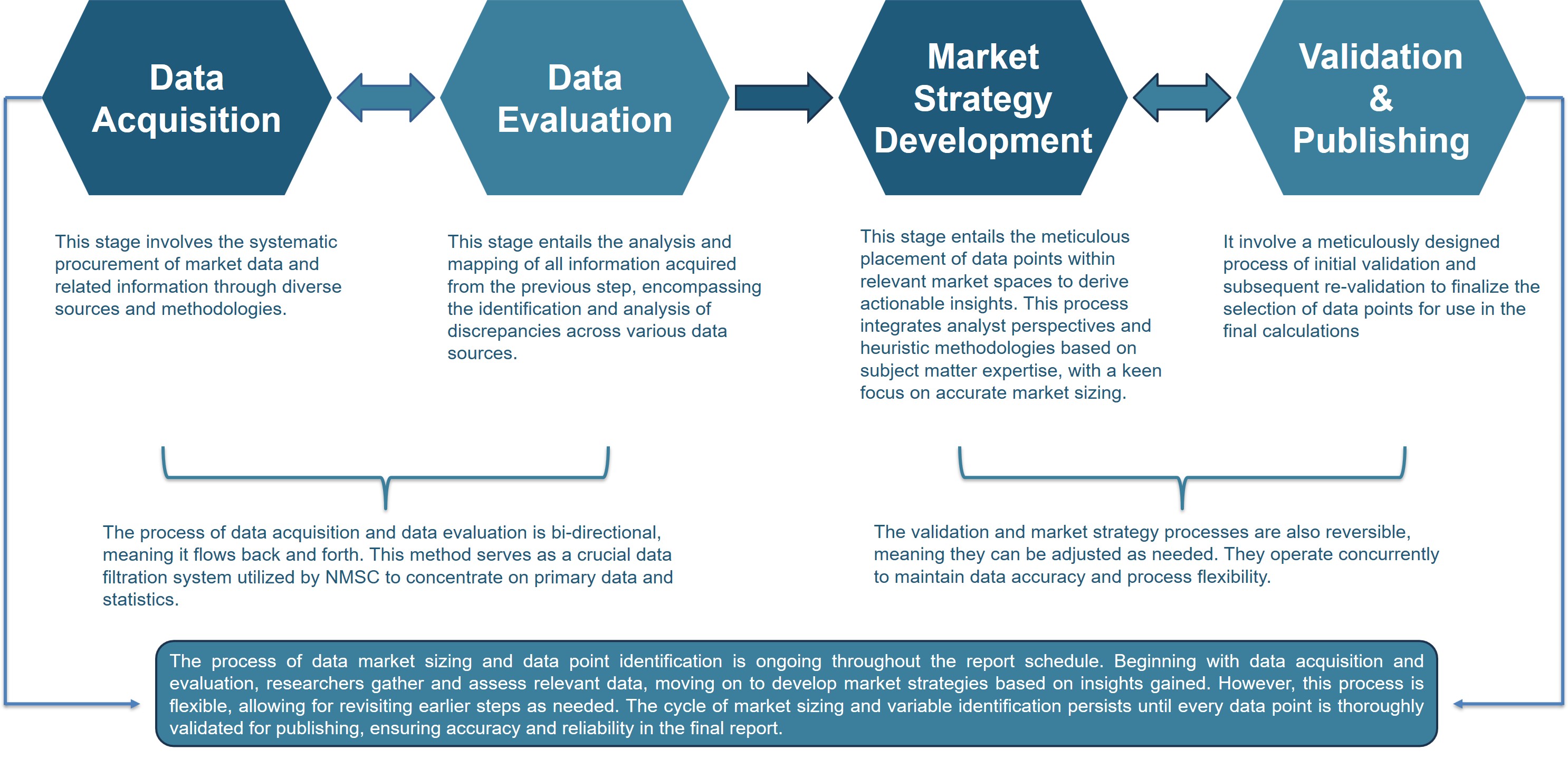
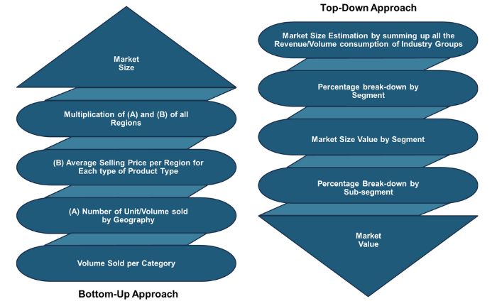
In-depth primary and secondary research; proprietary databases; rigorous quality control and validation measures. |
|
Analytical Tools |
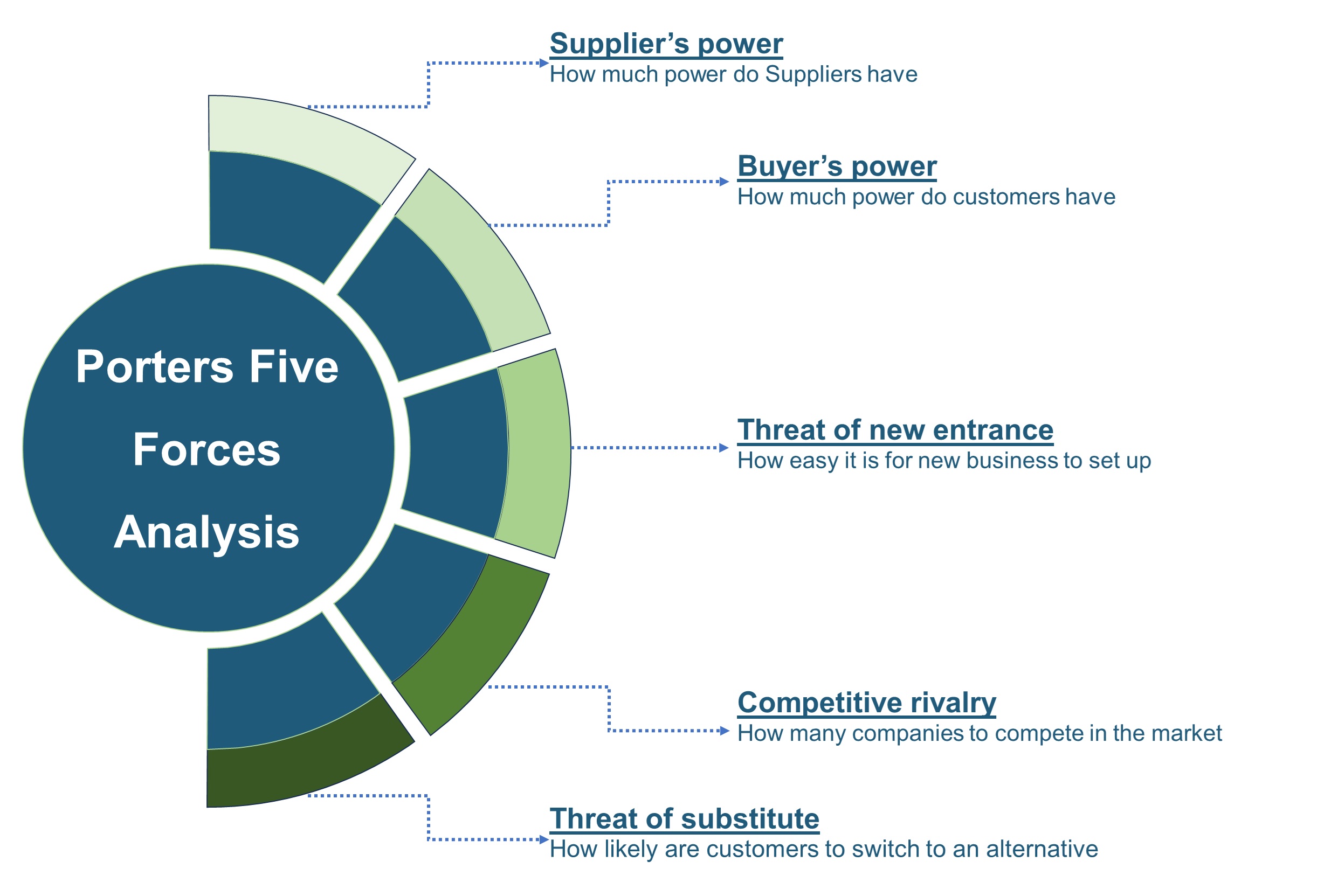
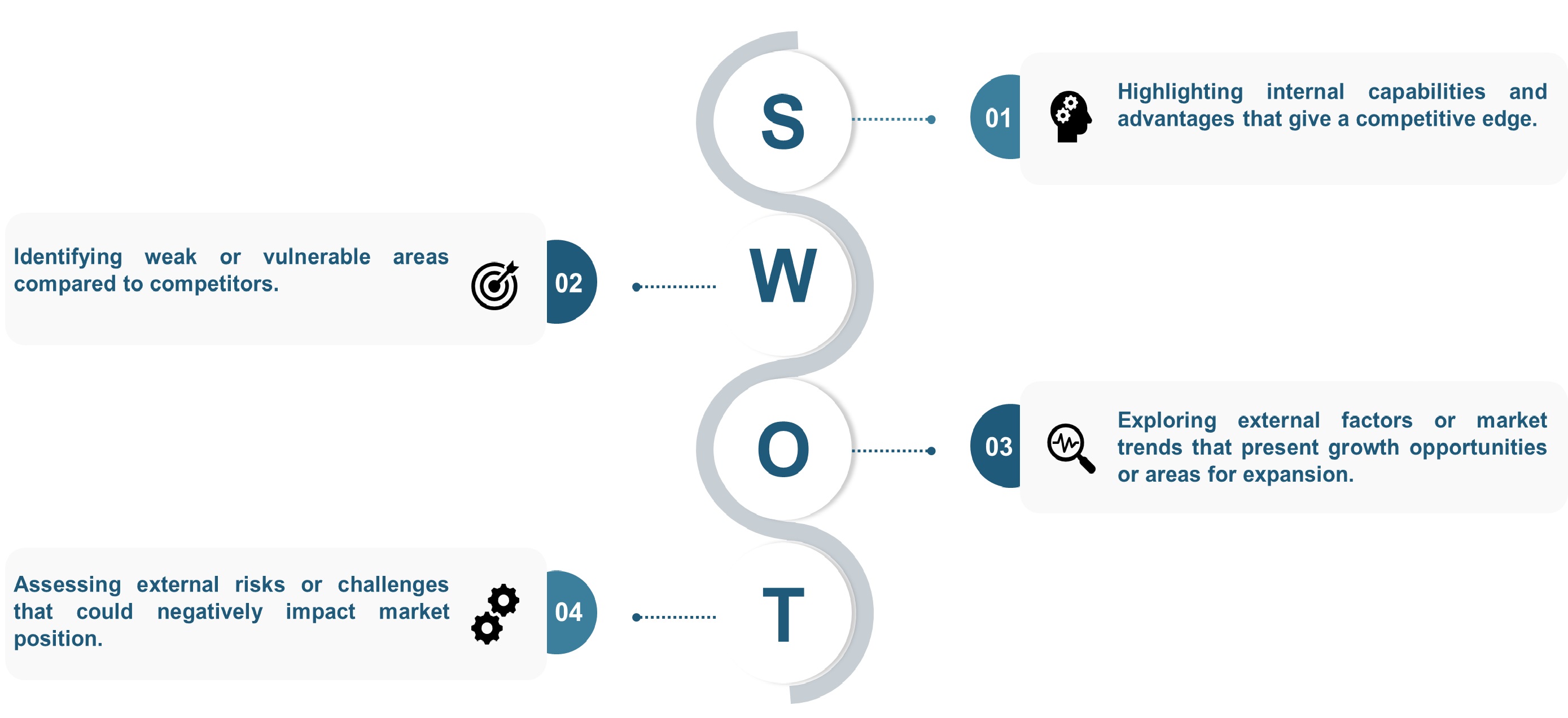
Porter's Five Forces, SWOT, value chain, and Harvey ball analysis to assess competitive intensity, stakeholder roles, and relative impact of key factors. |
Key Market Segments
By Integration Architecture
-
Monolithic Integration
-
Heterogeneous Integration
-
3D-Stacked Photonics
By Photonic Platform
-
Silicon Photonics (SiPh)
-
Indium Phosphide (InP)
-
Lithium Niobate on Insulator (LNOI)
-
Polymer / Other Emerging
By Modulation Scheme
-
Direct-Detect (NRZ, PAM-4)
-
Coherent (QPSK, QAM-16+)
By Performance Tier
-
Standard (<25 Gbps/lane)
-
Mid (25–100 Gbps)
-
High (>100 Gbps)
By Link Distance (µm-mm)
-
Intra-Die (<1 mm)
-
Inter-Die (1 mm–1 cm)
By Power Budget
-
Ultra-low (<1 pJ/bit)
-
Moderate (1–10 pJ/bit)
-
Standard (>10 pJ/bit)
By End-User
-
SoCs for HPC/AI
-
Network-on-Chip (NoC)
-
Memory Interfaces
-
Other Embedded
Geographical Breakdown
-
North America: U.S., Canada, and Mexico.
-
Europe: U.K., Germany, France, Italy, Spain, Sweden, Denmark, Finland, Netherlands, and rest of Europe.
-
Asia Pacific: China, India, Japan, South Korea, Taiwan, Indonesia, Vietnam, Australia, Philippines, and rest of APAC.
-
Middle East & Africa (MENA): Saudi Arabia, UAE, Egypt, Israel, Turkey, Nigeria, South Africa, and rest of MENA.
-
Latin America: Brazil, Argentina, Chile, Colombia, and rest of LATAM.
Conclusion & Recommendations
Our report equips stakeholders, industry participants, investors, policy-makers, and consultants, with actionable intelligence to capitalize on on-chip optical interconnect transformative potential. By combining robust data-driven analysis with strategic frameworks, NMSC’s on-chip optical interconnect market report serves as an indispensable resource for navigating the evolving landscape.






 Speak to Our Analyst


