Advanced Chip Packaging Market By Packaging Technology (2.5D Packaging, 3D Die-Stacking, and Others), By Integration Strategy (Monolithic Integration, Heterogeneous Multi-Die Integration, and Others), By Packaging Level (Component Level, System Level, and Sub-Assembly Level), By Interconnect Technology (TSVs, Micro-Bumps and Others), By Thermal Interface Materials (TIMs and Heat Spreaders), By End-User (Consumer Electronics, IT & Data Centers, and Others) – Global Analysis & Forecast, 2025–2035
Industry: Semiconductor & Electronics | Publishing Date: March 20, 2026 | Last Updated: March 20, 2026 | No of Pages: N/A | No. of Tables: N/A | No. of Figures: N/A | Format: PDF | Report Code: SE4310
Industry Outlook
The global Advanced Chip Packaging Market size was valued at USD 56.18 billion in 2025 and is expected to reach USD 62.31 billion by 2026. Looking ahead, the industry is projected to expand significantly, reaching USD 158.09 billion by 2035, registering a CAGR of 10.9% from 2026 to 2035.
Advanced Chip Packaging Market Size & Forecast
|
Parameters |
Details |
|
Market Size in 2026 |
USD 62.31 Billion |
|
Revenue Forecast in 2035 |
USD 158.09 Billion |
|
Growth Rate |
CAGR of 10.9% from 2026 to 2035 |
|
Analysis Period |
2025–2035 |
|
Base Year Considered |
2025 |
|
Forecast Period |
2026–2035 |
|
Market Size Estimation |
Billion (USD) |
|
Companies Profiled |
20 |
|
Countries Covered |
33 |
|
Market Share |
Available for 10 companies |
The advanced chip packaging market has evolved into a critical pillar of the global semiconductor industry by moving beyond its traditional role as a backend assembly function to become a strategic enabler of system-level performance. Based on our assessment of the current manufacturing landscape, this shift is primarily driven by the need to bypass the physical limitations of traditional silicon scaling.
Based on NMSC’s primary research, we have identified that advanced packaging now serves as the foundation for heterogeneous integration and chiplet-based architectures. These innovations allow for high-density interconnects that directly address modern power and form-factor constraints. We have observed these solutions being increasingly deployed across high-stakes applications such as artificial intelligence accelerators and data centre processors, where reliability and bandwidth optimisation are essential.
What are the Key Advanced Chip Packaging Industry Trends?
How are Heterogeneous Integration and Chiplet-Based Architectures Reshaping Advanced Packaging?
Based on our primary research and technical assessments across semiconductor manufacturing hubs in Asia-Pacific and North America, we observed that heterogeneous integration and chiplet-based architectures are fundamentally reshaping the advanced chip packaging landscape. We also found that advanced packaging has transitioned from a backend cost centre to a strategic enabler of system-level performance. Also, our evaluation of commercial deployments showed a higher adoption rate of 2.5D interposers, 3D IC stacking, and fan-out wafer-level packaging (FOWLP) to overcome the physical limitations of traditional monolithic scaling. Chiplet-based designs significantly improved yield economics and enable node-mixing flexibility, particularly for high-performance computing (HPC) and AI accelerators.
How are AI, HPC, and Automotive Workloads Driving Demand for High-Density and High-Performance Packaging?
Our primary research with semiconductor manufacturers and OEMs indicates that rapid growth in AI training, HPC, cloud data centers, and ADAS is significantly accelerating demand for advanced packaging. As AI models scale from training to large-scale inference, conventional packaging technologies are struggling to meet rising power density, bandwidth, and latency requirements. This is driving adoption of high-density interconnects, heterogeneous integration, and chiplet-based architectures to enable faster data transfer and improved thermal performance.
In automotive applications, the shift toward 800-volt EV platforms and autonomous computing is reinforcing the need for thermally robust, high-reliability packaging solutions with long product lifecycles. However, despite strong demand momentum, supply constraints in advanced substrates and backend capacity continue to limit near-term scalability across the ecosystem.
How are Software-Driven Design Enablement and Co-Optimisation Enhancing Advanced Packaging Adoption?
Our discussions with system architects indicate that software-driven design enablement is emerging as a key catalyst for advanced packaging adoption. Early-stage co-design across silicon, package, and system layers is reducing integration complexity and improving architectural alignment. Implementation assessments show that chip-package co-design (CPCD) tools, along with thermal simulation, signal integrity analysis, and power delivery modelling platforms, are significantly lowering design risk while accelerating validation cycles.
Companies adopting software-first methodologies report higher first-pass silicon success and faster time-to-market, reflecting a broader industry shift toward integrated digital engineering frameworks. However, limited interoperability and a lack of standardisation across design tools and IP ecosystems continue to restrict seamless collaboration, posing scalability challenges for widespread advanced packaging deployment.
SWOT Analysis of the Advanced Chip Packaging Industry:
The advanced chip packaging market is rapidly evolving, driven by demand for high-performance, miniaturised, and energy-efficient semiconductor solutions across key technology sectors.

The advanced chip packaging market is experiencing rapid growth, driven by the increasing demand for high-performance, miniaturised, and energy-efficient semiconductor solutions across AI, high-performance computing (HPC), automotive, IoT, and telecommunications sectors. Its strengths lie in the ability to deliver advanced, compact, and energy-efficient packaging solutions that significantly enhance semiconductor performance.
However, the market faces weaknesses related to high manufacturing and R&D costs, largely due to complex fabrication processes and the use of specialised materials. At the same time, substantial opportunities are emerging as technological advancements and expanding applications create demand for innovative packaging architectures. Conversely, stringent regulatory standards and reliability requirements, particularly for critical applications, present ongoing threats. Understanding these factors is essential for industry stakeholders to effectively manage challenges, capitalise on growth opportunities, and sustain competitiveness in this rapidly evolving advanced chip packaging market.
What Are the Key Market Drivers, Breakthroughs, And Investment Opportunities that Will Shape the Advanced Chip Packaging Industry in the Next Decade?
Growth Catalyst & Risk Assessment Matrix
|
DRIVERS/TRENDS/RESTRAINTS |
(+/-) % IMPACT ON THE CAGR FORECAST |
GEOGRAPHIC RELEVANCE |
IMPACT TIMELINE |
|
Rising demand for high-performance computing (HPC), AI, and data-centre chips is driving the adoption of advanced packaging technologies (2.5D/3D ICs, CoWoS, FOWLP) |
+0.9% |
Global, strongest in Asia Pacific (Taiwan, South Korea), North America |
Short to medium term (≤ 3 years) |
|
Increasing integration of heterogeneous chips (logic, memory, analog) is boosting demand for system-in-package (SiP) and chiplet-based architectures |
+0.8% |
North America, Asia Pacific, and growing adoption in Europe |
Medium term (2–4 years) |
|
Miniaturisation and power-efficiency requirements in consumer electronics, automotive electronics, and IoT are accelerating the use of advanced wafer-level and fan-out packaging |
+0.7% |
Global, the highest impact in Asia Pacific and Europe |
Short to medium term (≤ 3 years) |
|
Expansion of advanced packaging capacity by foundries and OSATs, supported by government semiconductor initiatives and investments |
+0.6% |
Asia Pacific, North America, Europe (CHIPS Act regions) |
Medium to long term (2–5 years) |
|
High capital expenditure, yield challenges, and complex supply chains associated with advanced packaging processes are constraining adoption |
–0.7% |
Global, most pronounced in emerging semiconductor regions |
Medium term (2–4 years) |
Our research and market evaluations indicate that the advanced chip packaging market is being driven by structural shifts in semiconductor supply chains and rising system-level design complexity. Specifically, supply-chain localisation efforts and geopolitical risk mitigation strategies are positioning advanced packaging as strategic infrastructure, supported by government incentives, regional backend capacity expansion, and stringent reliability requirements in defence and automotive applications, which collectively sustain demand for advanced packaging equipment, materials, and services.
Simultaneously, increasing system complexity and multi-die integration across AI, automotive, networking, and industrial electronics are raising packaging content per device, accelerating the adoption of high-density and thermally efficient packaging formats and supporting advanced chip packaging market growth even amid semiconductor volume fluctuations. However, high capital intensity, manufacturing complexity, and prolonged yield learning cycles continue to constrain adoption, particularly among mid-tier and regional players.
Growth Drivers:
How are Supply-Chain Localisation and Backend Capacity Expansion Driving Advanced Chip Packaging Sales and Consumption?
Based on our primary research across semiconductor supply chains, supply-chain localisation and backend capacity expansion are materially driving 2.5D packaging sales and consumption. OSAT executives emphasised that advanced packaging is increasingly treated as strategic infrastructure rather than a cost-optimised backend function, prompting government-backed semiconductor programs to subsidise domestic capacity and encourage regional manufacturing. OEMs are also dual-sourcing and regionalising backend operations to mitigate geopolitical risks and ensure secure, traceable packaging flows for regulated sectors such as automotive and defence. Foundries and OSATs are accelerating facility expansions to align with local advanced-node fabs, directly increasing packaging volumes and value capture. However, while localisation strengthens resilience and compliance, it raises per-unit costs and exposes shortages of specialised engineering talent, making backend expansion both a growth catalyst and an operational constraint shaping market adoption.
How is Rising System-Level Complexity and Multi-Die Integration Increasing Advanced Chip Packaging Consumption?
Rising system-level complexity and multi-die integration are structurally increasing chiplet architecture consumption across AI, automotive, networking, and industrial applications. Based on our assessment, modern semiconductor designs increasingly integrate multiple logic, memory, analogue, and power dies within compact form factors, directly expanding packaging content per device. As architectures become more heterogeneous, multi-die configurations raise the number of advanced packages per system, while higher interconnect density requirements accelerate adoption of fan-out and 2.5D/3D packaging technologies. Tighter thermal and power constraints are further driving demand for advanced substrates, interposers, and specialised materials, increasing design and manufacturing complexity. Additionally, application-specific customisation is elevating per-unit packaging value. As a result, advanced packaging consumption continues to grow even during semiconductor volume fluctuations, reinforcing its role as a structural, rather than purely cyclical, market driver.
Growth Inhibitors:
How are High Capital Intensity and Manufacturing Complexity Constraining Advanced Chip Packaging Adoption?
High capital intensity and manufacturing complexity are materially constraining advanced chip packaging adoption. Our evaluation of industry investments indicates that advanced packaging requires substantial upfront expenditure in specialised equipment, cleanroom expansion, and continuous process R&D, creating significant entry barriers for mid-tier and regional players. As a result, capacity expansion remains concentrated among a limited number of large foundries and OSAT providers, restricting broader ecosystem participation.
In addition, advanced packaging processes demand stringent process control, specialised materials, and highly skilled engineering talent, increasing execution risk and extending project timelines. Prolonged yield ramp-up cycles and thermal-mechanical reliability challenges further delay time-to-volume production. Collectively, these capital and operational constraints slow capacity build-outs and limit near-term scalability, reinforcing manufacturing complexity as a critical inhibitor to advanced chip packaging market expansion.
Growth Opportunities:
How are the Expansion of Chiplet Ecosystems and Design Enablement Platforms Creating New Advanced Chip Packaging Market Growth Opportunities?
The expansion of chiplet ecosystems and design enablement platforms is unlocking significant growth opportunities in advanced chip packaging. Our analysis indicates that standardised chiplet architectures and integrated co-design workflows are reducing development risk, improving design reuse, and accelerating commercialisation, thereby increasing industry confidence in advanced packaging adoption. Fabless semiconductor firms highlighted that standardised chiplet interfaces enable modular system architectures, lowering integration complexity and shortening product development cycles.
Additionally, packaging-aware design tools, open interconnect standards, and closer foundry–OSAT collaboration models are supporting phased deployment strategies, allowing companies to scale advanced packaging without incurring excessive upfront capital exposure. Early adopters leveraging modular chiplet strategies have demonstrated faster time-to-market and enhanced product flexibility across AI, automotive, and networking applications. However, broader ecosystem interoperability and industry-wide standardisation remain critical to fully scaling chiplet-driven packaging growth.
How Advanced Chip Packaging Industry Segmented in this Report, and What are the Key Insights from the Segmentation Analysis?
Market Highlights & Strategic Insights – Advanced Chip Packaging Market:
|
Segments |
Key Takeaways |
|
Packaging Technology |
2.5D packaging dominates within advanced packaging due to its strong adoption in AI accelerators, HPC processors, and multi-chip modules. 3D die-stacking is the fastest-growing segment, driven by HBM integration, memory-on-logic architectures, and increasing demand for ultra-high bandwidth solutions. System-in-Package (SiP) and MCM solutions are expanding for heterogeneous integration, while legacy advanced packages remain relevant in cost-sensitive applications. |
|
Integration Strategy
|
Monolithic integration dominates as single-die, node-scaled designs still account for the majority of chip production. However, modular chiplet-based integration is witnessing the highest growth due to design flexibility, improved yields, heterogeneous integration, and rising AI/data centre demand. |
|
Packaging Level |
Component-level packaging dominates since most semiconductors are individually packaged. Sub-assembly and system-level packaging are growing rapidly due to increasing adoption of multi-die modules, chiplets, and fully integrated heterogeneous compute platforms. |
|
Component Type |
Processing ICs and memory ICs account for the largest share of packaging demand, supported by high production volumes and performance-intensive applications. Memory ICs, particularly high-bandwidth memory (HBM), are experiencing the fastest growth due to AI workloads and data center expansion. Mixed-signal, RF, power devices, optoelectronics, and MEMS are expanding across automotive, IoT, and telecom sectors. |
|
Performance |
High-performance computing (HPC) dominates demand, particularly in AI accelerators, servers, and cloud data centers. High-bandwidth memory solutions represent the fastest-growing performance segment. Low-power, high-frequency, and secure packaging solutions are gaining traction in mobile, automotive, industrial, and defense applications. |
|
Substrate Type |
Organic substrates (ABF, BT resin) dominate due to cost efficiency and scalability. Silicon and glass interposers are the fastest-growing substrate segments, driven by AI, HPC, and advanced 2.5D/3D architectures. Ceramic and flexible substrates are used in high-reliability and specialised applications. |
|
End-User |
Consumer electronics and IT/data centers dominate volume. Automotive, telecom/5G infrastructure, industrial IoT, aerospace, healthcare, and robotics are high-growth areas due to performance, reliability, and miniaturisation demands. |
By Packaging Technology Insights
How Did Packaging Technology Choices Shape the Advanced Chip Packaging Market Share?
Based on the packaging technology, the advanced chip packaging market is segmented into 2.5D packaging, 3D Die-Stacking, System-in-Package (SiP), Chip-on-Board (CoB), and Legacy Advanced Packages
From our assessment of integration strategies, we observed that each technology addresses distinct performance, density, and cost requirements. 2.5D packaging has gained strong adoption in AI and high-performance computing applications due to its ability to integrate heterogeneous dies with high-bandwidth interconnects. 3D die-stacking further enhances performance by vertically integrating memory and logic, improving bandwidth density and power efficiency for data-intensive workloads. SiP solutions enable compact, multifunctional integration for mobile, automotive, and IoT systems, while CoB remains relevant for space-efficient and cost-sensitive designs. Legacy advanced packages continue to support high-volume consumer and industrial applications. Overall, packaging technology selection is increasingly driven by workload demands, thermal constraints, and system-level co-design considerations rather than standalone chip performance requirements.
By Packaging Level Insights
How Did Packaging Levels Across the System Hierarchy Shape the Advanced Chip Packaging Market?
On the basis of packaging level, the advanced chip packaging market is segmented into component level, sub-assembly level, and system level.
From our evaluation of system integration programs, we found that packaging decisions at each hierarchy level are addressed with distinct integration, performance, and reliability requirements. Our discussions with system packaging engineers indicated that component-level packaging primarily focused on die protection, interconnect density, and thermal performance to ensure device-level functionality and reliability. Building on this, sub-assembly-level packaging enabled functional grouping and modular integration of multiple packaged components, supporting scalable system architectures and improving design flexibility.
At the system level, advanced packaging facilitated higher degrees of functional consolidation, space optimisation, and power management within complete electronic assemblies. Overall, we observed that selection across packaging levels was increasingly influenced by holistic system architecture considerations, lifecycle requirements, and co-design strategies rather than isolated component-level decisions, reinforcing the shift toward system-centric packaging design approaches.

By Substrate Insights
How did Substrate and Material Choices Influence the Advanced Chip Packaging Market Demand?
On the basis of the Substrate, the advanced chip packaging market is segmented into organic substrates, silicon interposers, glass interposers, ceramic substrates and flexible substrates.
From our evaluation, we observed that organic substrates dominate due to their cost efficiency, scalability, and widespread use in high-volume consumer and computing applications. However, silicon interposers are increasingly adopted in 2.5D and 3D architectures to enable high-density interconnects and superior electrical performance for AI and high-performance computing workloads. Glass interposers are emerging as a promising alternative, offering improved dimensional stability and fine-line routing capabilities. Ceramic substrates continue to serve high-reliability and high-temperature environments such as aerospace and automotive, while flexible substrates support compact and lightweight designs in wearable and specialised electronics. Overall, substrate selection is increasingly influenced by bandwidth requirements, thermal management needs, reliability standards, and system-level integration strategies.

Regional Outlook
Geographic Performance Snapshot:
|
Geography |
Key Takeaways |
|
North America |
A technology-driven and innovation-led market, supported by strong demand from AI, high-performance computing, data centers, aerospace & defense, and advanced automotive electronics. Growth is fueled by heavy R&D investments, government-backed semiconductor initiatives, and early adoption of advanced packaging technologies such as 2.5D, 3D, chiplets, and heterogeneous integration. |
|
Europe |
Growth is shaped by a strong focus on automotive electronics, industrial automation, and high-reliability applications. European advanced chip packaging market emphasise energy-efficient, trusted, and automotive-grade packaging solutions, supported by regional semiconductor initiatives and increasing investments in advanced packaging capabilities aligned with sustainability and supply-chain resilience goals. |
|
Asia‑Pacific |
Largest and fastest-growing advanced chip packaging market due to the concentration of foundries and OSATs, high-volume consumer electronics production, and rapid adoption of 5G, AI, and EV technologies. Strong demand for fan-out wafer-level packaging, flip-chip, and 2.5D/3D integration across China, Taiwan, South Korea, Japan, and Southeast Asia drives scale, cost efficiency, and continuous innovation. |
|
Latin America |
Emerging market growth is supported by expanding telecom infrastructure, IoT adoption, and automotive electronics demand, particularly in Brazil and Mexico. The region has limited local advanced packaging capacity, with growth largely driven by increased consumption of packaged semiconductor devices and gradual integration into global semiconductor supply chains. |
|
Middle East & Africa |
Early-stage adoption driven by investments in digital infrastructure, telecom, defense, smart cities, and data centers. Demand centers around high-performance and reliable semiconductor solutions, while local advanced packaging manufacturing remains limited. Government-led diversification initiatives support long-term growth despite developing regulatory and ecosystem maturity. |
The advanced chip packaging market is geographically studied across North America, Europe, Asia Pacific, the Middle East & Africa, and Latin America, and each region is further studied across countries.
Advanced Chip Packaging Market in North America
North America represents a design-led and strategically driven advanced chip packaging region, supported by strong R&D capabilities, government-backed semiconductor programs, and high-value end markets such as AI, defense, and data centres. Based on NMSC’s regional assessments, North America accounted for a significant share of global advanced packaging demand in 2025, driven primarily by the United States. The region benefits from global leadership in advanced chip design and increasing backend localisation initiatives aimed at strengthening supply-chain resilience. Our analysis shows that regional demand is skewed toward high-performance packaging formats, including 2.5D/3D ICs, advanced substrates, and HBM integration, with buyers prioritising reliability, security, and long-term supply assurance over cost optimisation.
Advanced Chip Packaging Market in the United States
The United States remained the largest contributor to advanced chip packaging demand, driven by AI accelerators, cloud infrastructure, aerospace, and defense electronics. Based on our engagements with OSAT partners, adoption is strongly influenced by CHIPS Act incentives and national security considerations, which are accelerating domestic packaging investments. The U.S. advanced chip packaging market increasingly treats advanced packaging as an extension of frontend technology development, with rising investments in chiplet architectures, heterogeneous integration, and co-design platforms. However, while domestic backend capacity is expanding, reliance on international OSATs persists, reinforcing the need for strategic partnerships and long-term capacity agreements to ensure supply continuity.
Advanced Chip Packaging Market in Canada
Canada represents a smaller but strategically relevant advanced chip packaging market, primarily supported by strong research institutions, automotive electronics initiatives, and speciality semiconductor applications. Based on our research, we found that demand for advanced packaging in Canada is concentrated in power electronics, sensing, and industrial applications, where buyers prioritise reliability, qualification standards, and collaborative R&D models rather than high-volume manufacturing. In this context, government-backed innovation programs are playing a critical role in supporting early-stage packaging development and materials research, while Canada’s close proximity to U.S. semiconductor supply chains facilitates cross-border collaboration and technology transfer. As a result, Canada is emerging as a complementary innovation- and materials-focused ecosystem within the broader North American advanced chip packaging landscape, supporting regional R&D, substrate development, and specialised application-driven packaging requirements.
Advanced Chip Packaging Market in Europe
Europe accounted for a moderate but structurally resilient share of global advanced chip packaging demand, shaped by regulation-driven adoption patterns and a strong concentration of automotive and industrial end markets. Based on our regional analysis, we observed that reliability, functional safety, and sustainability requirements significantly influence packaging technology selection across the region. Advanced packaging adoption is primarily driven by automotive electronics, industrial automation, power semiconductors, and aerospace applications, where long product lifecycles and certification standards are critical. In this context, Europe’s fragmented manufacturing ecosystem has increased reliance on collaborative partnerships among OSATs, research institutes, and system OEMs, reinforcing demand for certified, long-lifecycle packaging solutions rather than rapid technology turnover.
Advanced Chip Packaging Market in the United Kingdom
Within this regional landscape, the United Kingdom represents a design- and innovation-oriented advanced chip packaging market, supported by strong fabless activity, leading research institutions, and defense-focused applications. Our research shows an increasing emphasis on chiplet architectures, advanced interconnects, and packaging-aware design workflows, reflecting the UK’s strategic focus on system design, semiconductor IP, and early-stage technology development. However, large-scale manufacturing capacity remains limited, positioning the UK primarily as a design enablement and innovation hub rather than a volume manufacturing center. As a result, buyers in the UK prioritise security, performance optimisation, and collaborative development models over scale-driven manufacturing economics.
Advanced Chip Packaging Market in Germany
Germany exhibits an engineering-led and quality-centric adoption pattern, driven by its strong automotive electronics, industrial automation, and power semiconductor industries. Our research indicates robust demand for advanced packaging solutions that deliver thermal reliability, mechanical robustness, and automotive-grade qualification, aligning with Germany’s focus on mission-critical industrial and mobility systems. Consequently, buyers prioritise certifications, long-term vendor relationships, and process transparency, which support premium deployments and sustained supplier engagement across the automotive and industrial value chain.
Advanced Chip Packaging Market in France
Similarly, France demonstrates steady growth in advanced chip packaging demand, supported by aerospace, defense, automotive, and industrial electronics applications. Advanced packaging adoption is reinforced by public–private R&D initiatives and national semiconductor strategies aimed at strengthening domestic technology sovereignty. In this environment, buyers emphasise regulatory compliance, data sovereignty, and supply-chain transparency, favouring vendors with strong local partnerships and qualification expertise. Consequently, reliability and security considerations outweigh cost-driven decision-making, reinforcing France’s positioning as a sovereignty- and mission-critical–driven advanced chip packaging market within Europe.
Advanced Chip Packaging Market in Italy
Within Southern Europe, Italy represents a niche but expanding advanced chip packaging market, supported by its strong industrial electronics base, automotive supply chains, and power device applications. Based on our analysis, we observed that demand is concentrated on advanced substrates, module-level packaging, and application-specific customisation to support specialised industrial and automotive use cases. Italian buyers prioritise flexibility, close design collaboration, and integration support, reflecting the country’s focus on customised system development rather than high-volume semiconductor manufacturing.
Advanced Chip Packaging Market in Spain
Similarly, Spain is witnessing the gradual adoption of advanced chip packaging, driven by industrial electronics, automotive components, and emerging national semiconductor initiatives. Our research indicates that demand in Spain is focused on packaging solutions that balance performance enhancement with cost efficiency, aligning with the country’s emphasis on competitive manufacturing and system integration. Furthermore, buyers are increasingly interested in modular and scalable packaging approaches, particularly where integration with broader European supply chains and research programs is feasible, reinforcing Spain’s role as a cost-performance-oriented adoption market within Europe.
Advanced Chip Packaging Market in the Nordics
In contrast, the Nordic countries represent high-value, low-volume adopters of advanced chip packaging, driven by telecommunications, industrial automation, and power electronics applications. Our research indicates a strong emphasis on energy efficiency, sustainability, and long-term system reliability, which significantly influences packaging technology selection. Consequently, buyers favour advanced substrates, thermal management solutions, and vendors offering comprehensive lifecycle support and environmental compliance, positioning the Nordics as sustainability- and reliability-focused advanced packaging adopters within the European semiconductor ecosystem.
Advanced Chip Packaging Market in the Asia-Pacific
Asia-Pacific represents the global manufacturing and commercialisation hub for advanced chip packaging, supported by dense foundry and OSAT ecosystems, extensive supply-chain integration, and strong government backing across major semiconductor economies. Based on our analysis, we observed that the region leads in both technology deployment and manufacturing scale, serving large-scale demand from AI, consumer electronics, automotive, and networking markets. In addition, close integration between frontend wafer fabrication and backend packaging operations accelerates technology innovation, reduces time-to-market, and supports rapid capacity expansion, reinforcing Asia-Pacific’s dominant position in the global advanced packaging value chain.
Advanced Chip Packaging Market in China
Within the Asia-Pacific region, China represents a scale-driven and rapidly expanding advanced chip packaging market, supported by aggressive domestic semiconductor investments and backend localisation initiatives. Our research indicates strong demand for fan-out, substrate-based, and multi-die packaging technologies across consumer electronics, AI hardware, and networking equipment, reflecting China’s large-volume system manufacturing base. Domestic OSATs play a central role in meeting this demand, while national technology self-sufficiency objectives and cost competitiveness significantly shape adoption strategies. Consequently, China is emerging as a high-volume advanced packaging manufacturing and commercialisation center within the regional ecosystem.
Advanced Chip Packaging Market in Japan
Japan demonstrates precision- and reliability-led adoption of advanced chip packaging, supported by its strengths in automotive electronics, industrial manufacturing, and advanced materials. Our observations show strong demand for advanced substrates, high-reliability interconnects, and process-controlled packaging solutions, aligning with Japan’s focus on high-performance and mission-critical applications. As a result, buyers prioritise quality assurance, long-term supplier relationships, and manufacturing consistency over rapid scaling, positioning Japan as a high-value, quality-centric advanced chip packaging market within the Asia-Pacific region.
Advanced Chip Packaging Market in India
India represents an emerging and strategically important advanced chip packaging market, driven by national semiconductor policy initiatives and the expansion of domestic electronics manufacturing. Based on our research, we observed early-stage adoption concentrated on OSAT development, assembly, testing, and automotive-grade packaging capabilities, reflecting India’s current focus on backend ecosystem creation. While the advanced packaging ecosystem remains under development, long-term market potential is supported by rising domestic electronics demand and government-backed incentive programs, positioning India as a future growth-oriented backend manufacturing and services hub in the region.
Advanced Chip Packaging Market in South Korea
In contrast, South Korea represents an advanced adopter of chip packaging technologies, supported by vertically integrated semiconductor ecosystems and strong leadership in memory and AI-driven architectures. Our analysis shows a strong emphasis on advanced interposers, memory stacking, and high-performance packaging solutions, driven by leading memory and logic manufacturers. Furthermore, rapid technology adoption and close coordination between design, manufacturing, and packaging teams enable accelerated commercialisation of next-generation packaging architectures, positioning South Korea as a technology execution-driven advanced chip packaging market within Asia-Pacific.
Advanced Chip Packaging Market in Taiwan
Taiwan represents the global nucleus of advanced chip packaging innovation and execution, underpinned by deep integration among leading foundries, OSATs, materials suppliers, and equipment vendors. Based on NMSC’s ecosystem-level evaluations, we observed that advanced packaging in Taiwan is treated as a core component of semiconductor process co-optimisation rather than a downstream activity. Our further engagements with industry participants indicated that buyers prioritise throughput stability, yield learning acceleration, and packaging-aware design enablement over cost considerations. The presence of dense supplier clusters supports rapid iteration cycles, while long-term capacity planning and capital commitments reinforce Taiwan’s position as the global reference market for leading-edge advanced packaging.
Advanced Chip Packaging Market in Indonesia
Indonesia remains at an early but structurally developing stage of advanced chip packaging adoption, shaped primarily by its role within the broader Southeast Asian electronics manufacturing and backend services ecosystem. From our regional assessments, we observed growing interest in OSAT-related activities, particularly assembly, testing, and substrate-adjacent operations, driven by multinational electronics manufacturers pursuing geographic risk diversification. Our interactions with stakeholders revealed that workforce capability development, infrastructure readiness, and technology transfer partnerships are central to market progression. Consequently, vendors entering Indonesia are increasingly emphasising phased investments, training programs, and collaboration with regional integrators, positioning Indonesia as a long-term backend expansion node rather than a near-term advanced packaging innovation hub.
Advanced Chip Packaging Market in Australia
Australia represents a specialised and application-driven advanced chip packaging market, supported by defense electronics, aerospace systems, industrial automation, and research-intensive semiconductor programs. Based on NMSC’s market engagements, we observed that adoption is highly selective and primarily driven by mission-critical requirements, with strong emphasis on reliability, security, and performance validation rather than manufacturing scale. As a result, advanced packaging solutions are mainly consumed in niche, high-value applications that require extended lifecycle support and compliance with stringent qualification standards. Collaboration among universities, government research agencies, and international semiconductor partners plays a central role in enabling technology transfer and adoption. Consequently, vendors offering deep technical support, customisation capabilities, and long-term engagement models are better positioned to succeed in the Australian advanced packaging ecosystem.
Advanced Chip Packaging Market in Latin America
Latin America represents a selective and emerging advanced chip packaging market, influenced by automotive electronics, industrial manufacturing, and regional electronics assembly activities. Our analysis indicates that adoption remains application-specific, with demand focused on backend operations, module-level packaging, and regional supply-chain participation rather than leading-edge packaging technologies. Economic volatility, infrastructure disparities, and capital constraints continue to influence investment pacing and technology adoption timelines. However, our engagements with industry participants indicate growing interest in supply-chain diversification and nearshoring, particularly among global OEMs serving the Americas. Accordingly, vendors that align with local manufacturing ecosystems, offer flexible engagement models, and support gradual capability development are more likely to capture sustainable long-term opportunities in the region.
Advanced Chip Packaging Market in the Middle East & Africa
The Middle East & Africa region presents a dual-speed advanced chip packaging landscape, characterised by selective high-value adoption in parts of the Middle East and nascent development across much of Africa. Based on our regional assessments, we observed that Middle Eastern markets are prioritising strategic semiconductor initiatives linked to defense, industrial digitisation, and national technology diversification agendas, which are driving targeted adoption of advanced packaging solutions. In these advanced chip packaging markets, buyers emphasise reliability, security, and long-term capacity assurance, typically supported through international partnerships and government-led programs.
In contrast, Africa remains at an early stage of adoption, with limited direct demand but increasing interest associated with infrastructure development and electronics assembly activities. Therefore, vendors pursuing this region must adopt differentiated strategies, including premium, partnership-driven approaches in the Middle East and capability-building, service-oriented models in Africa, to unlock long-term growth potential.
Competitive Landscape
Competitive Dynamics & M&A Landscape:
|
Key Takeaways |
|
The advanced chip packaging market comprises a combination of large, globally dominant OSATs and integrated semiconductor leaders such as ASE, Amkor Technology, Intel Corporation, Samsung, GlobalFoundries, UMC, Micron Technology, Texas Instruments, UTAC, and NXP Semiconductors, alongside highly specialised and regionally focused providers including Powertech Technology Inc. (PTI), Tongfu Microelectronics, Hana Micron, ChipMOS, King Yuan Electronics (KYEC), Silicon Box, Nepes, Deca Technologies, and JCET-linked entities, which support high-density, high-reliability, and next-generation packaging requirements. |
|
Market participants are adopting a strategic mix of 2.5D and 3D IC integration, chiplet-based architectures, fan-out wafer-level and panel-level packaging, heterogeneous integration, and advanced thermal and interconnect solutions to enhance performance, power efficiency, and miniaturisation. These strategies are aligned with rising demand from AI accelerators, high-performance computing, automotive electronics, 5G infrastructure, data centers, and advanced consumer devices, where packaging plays a critical role in system-level performance. |
|
Recent investments, partnerships, and capacity expansions focus on strengthening advanced packaging capabilities, expanding geographic manufacturing footprints, and improving supply-chain resilience, particularly across the Asia Pacific and North America. Leading players are prioritising new advanced packaging lines, proprietary process development, and ecosystem collaborations to support scaling beyond Moore’s Law and to secure competitive positioning in high-growth, technology-intensive semiconductor applications. |
Which Companies Dominate the Advanced Chip Packaging Industry and How do they Compete?
From our research, leading players such as Intel Corporation, Samsung, GlobalFoundries, Amkor Technology, ASE, and JCET Group compete across design, fabrication, advanced packaging, and testing. Authoritative manufacturers like Intel and Samsung leverage vertically integrated models and decades of process know-how to maintain performance leadership. In contrast, experienced OSAT specialists, including Amkor, ASE, and Powertech Technology, focus on advanced packaging, fan-out, and heterogeneous integration, supporting fabless and IDM customers. Trust and credibility in this advanced chip packaging market are built through long-term customer relationships, proven yield performance, and compliance with global quality standards. Overall, competition is driven by demonstrated manufacturing reliability, technological depth, and the ability to scale advanced packaging for AI, HPC, and automotive demand.
Market Dominated by Advanced Chip Packaging Giants and Specialists
The advanced chip packaging market is shaped by powerhouse manufacturers and niche specialists. Established giants such as Intel and Samsung leverage scale, while outsourced semiconductor assembly and test (OSAT) leaders like Amkor Technology and ASE dominate packaging and backend services. Mid-tier players such as JCET, Powertech Technology, and ChipMOS Technologies carve out niches in specific technologies and regional markets. The diverse competitive landscape fosters deep specialisation, global networks in the Asia Pacific integrate manufacturing and packaging, while U.S. firms emphasise design innovation and foundry support. This balance between broad capabilities and targeted expertise sustains market dynamism and keeps competition alive across states, end uses, and supply chain segments.
Innovation and Adaptability Drive Market Success
Innovation remains the heartbeat of success in the advanced chip and packaging market. Leaders like Intel and Samsung aggressively pursue heterogeneous integration, 3D packaging, and high-bandwidth memory solutions to outpace rivals. For example, Amkor’s groundbreaking advanced packaging facilities in Arizona signal a strategic pivot toward U.S., led packaging capabilities, tied to CHIPS Act incentives and partnerships with high-profile customers like Apple and Nvidia. These moves boost adaptability in responding to rapid AI and HPC demand. Across the board, companies invest in process technologies and ecosystem partnerships to sustain competitiveness in emerging applications such as AI accelerators and automotive electronics.
Market Players to Opt for Merger & Acquisition Strategies to Expand their Presence
From our industry experience, M&A activity is a clear growth lever for advanced chip players. In 2025, GlobalFoundries recently acquired Singapore’s Advanced Micro Foundry to enhance its silicon photonics and AI-oriented portfolios, broadening its technology base. These real market moves illustrate how companies use M&A to accelerate innovation, expand market reach, and reshape competitive dynamics in advanced semiconductor tech
List of Key Advanced Chip Packaging Companies
-
Amkor Technology
-
GlobalFoundries
-
Intel Corporation
-
NXP Semiconductors
-
Powertech Technology Inc
-
JSCG
-
Tongfu Microelectronics Co., Ltd.
-
HANA Micron Inc.
-
Silicon Box Pte Ltd
-
CHIPBOND Technology Corporation
-
Deca Technologies
-
ChipMOS TECHNOLOGIES INC.
-
NEPES
-
ASE
-
UTAC
-
Texas Instrument Incorporated
-
King Yuan ELECTRONICS CO, LTD
-
United Microelectronics Corporation
What Are the Latest Key Industry Developments?
-
April 2025- Amkor and Intel EMIB packaging partnership announced that Amkor and Intel expanded Embedded Multi-Die Interconnect Bridge (EMIB) assembly capacity across Korea, Portugal, and the U.S., addressing growing heterogeneous integration demand for AI and high-performance systems.
-
February 2025- ASE Technology launched its fifth packaging plant in Malaysia. ASE Expanded its Chip Packaging and Testing Facility to Enable Next-Gen Applications.
What are the Key Factors Influencing Investment Analysis & Opportunities in the Advanced Chip Packaging Market?
Investment analysis in the advanced chip packaging market is increasingly shaped by its recognition as a strategic extension of front-end semiconductor manufacturing rather than a standalone backend service. Based on our ongoing engagement with investors, OSAT leadership, and technology suppliers, funding activity is concentrating on capacity expansion, process differentiation, and packaging-aware design capabilities. Valuations are being influenced by long-term customer commitments, proximity to advanced-node fabs, and demonstrated expertise in high-complexity packaging such as 2.5D, 3D, and fan-out architectures. Strategic and government-linked capital is playing a growing role, reflecting the market’s importance to supply-chain resilience and national technology agendas.
From an opportunity perspective, investment hotspots are emerging around regions that combine strong semiconductor ecosystems with policy support for backend localisation. Platforms enabling chiplet integration, advanced substrates, materials innovation, and co-design services are attracting sustained interest, as they address structural demand drivers rather than cyclical volume swings. Overall, investor focus is shifting toward scalable, ecosystem-embedded players positioned for long-term relevance.
Pain Point Analysis of the Advanced Chip Packaging Market:
The advanced chip packaging market is navigating a complex landscape driven by high costs, technological challenges, competitive pressures, and regional disparities.

The advanced chip packaging market is navigating a dynamic landscape, shaped by a combination of operational, technological, and regional challenges. High capital expenditure and substantial maintenance costs create significant financial barriers for companies seeking to adopt cutting-edge packaging equipment, while at the same time, customers demand faster time-to-market and express concerns regarding the reliability of newer technologies. This dual pressure compels vendors to balance speed with quality, intensifying competition among semiconductor foundries and service providers and driving continuous innovation, particularly in smaller nodes and heterogeneous integration solutions.
However, technological limitations, including dependence on legacy packaging lines and the complexity of implementing advanced thermal management, further constrain growth, creating gaps in service availability. These challenges are compounded by uneven adoption across end markets and limited access to high-end packaging services in emerging regions. Additionally, regional sensitivities, such as variations in labour and energy costs and disparities in semiconductor infrastructure, influence both cost competitiveness and scalability. Overall, we observed that companies in this market must strategically align innovation, operational efficiency, and regional adaptability to fully capitalise on the growing demand for advanced packaging solutions
Key Benefits for Stakeholders:
Next Move Strategy Consulting (NMSC) presents a comprehensive analysis of the advanced chip packaging market trends, covering historical trends from 2020 through 2025 and offering detailed forecasts through 2035. Our study examines the market at regional and country levels, providing quantitative projections and insights into key growth drivers, challenges, and investment opportunities across all major Advanced chip packaging segments.
The advanced chip packaging industry delivers differentiated value across its stakeholder ecosystem by aligning technical innovation with long-term strategic and commercial outcomes. From an investment perspective, the sector provides exposure to a structurally expanding segment of the semiconductor value chain that is increasingly decoupled from traditional wafer scaling cycles and supported by long-term capacity commitments, strategic partnerships, and policy-driven funding initiatives. For customers, including foundries, fabless semiconductor companies, and system OEMs, advanced packaging serves as a critical enabler of higher performance, accelerated time-to-market, and enhanced design flexibility through heterogeneous integration and chiplet-based architectures.
In parallel, equipment suppliers, materials vendors, and OSAT providers benefit from stronger customer lock-in, recurring revenue streams, and the ability to deliver higher value-added services beyond conventional backend processes. At the ecosystem level, governments and end users benefit from improved supply-chain resilience, enhanced product reliability, and strengthened capabilities to support next-generation applications across computing, automotive, and industrial domains. Collectively, these interlinked benefits position advanced chip packaging as a strategic pillar of the evolving semiconductor industry.
|
Parameters |
Details |
|
Customization Scope |
Free customization (equivalent to up to 80 analyst-working hours) after purchase. Addition or alteration to country, regional & segment scope. |
|
Pricing and Purchase Options |
Avail customized purchase options to meet your exact research needs. |
|
Approach |
In-depth primary and secondary research; proprietary databases; rigorous quality control and validation measures. |
|
Analytical Tools |
Porter's Five Forces, SWOT, value chain, and Harvey ball analysis to assess competitive intensity, stakeholder roles, and relative impact of key factors. |
Key Market Segments
By Packaging Technology
-
2.5D Packaging
-
Interposer-based 2.5D
-
Silicon Interposer
-
Glass Interposer
-
-
Bridge-based 2.5D
-
Embedded Silicon Bridge
-
Organic Bridge
-
-
-
3D Die-Stacking
-
TSV-based 3D
-
Memory-on-logic
-
Logic-on-logic
-
-
Hybrid-bonded 3D
-
Die-to-die (D2D)
-
Die-to-wafer (D2W)
-
Wafer-to-wafer (W2W)
-
-
-
System-in-Package (SiP)
-
Conventional SiP
-
Advanced SiP
-
Package-on-Package (PoP)
-
-
Multi-Chip Module (MCM)
-
Substrate-based MCM
-
Interposer-based MCM
-
-
Chip-on-Board (CoB)
-
Wire-bond CoB
-
Flip-chip CoB
-
-
Legacy Advanced Packages
-
Flip-Chip BGA
-
Fine-pitch Wire-bond Packages
-
By Integration Strategy
-
Monolithic Integration
-
Single-die packages
-
Node-scaled designs
-
-
Heterogeneous Multi-Die Integration
-
Logic + memory
-
Logic + analog / RF
-
Logic + power
-
-
Modular Chiplet-Based Integration
-
Compute chiplets
-
I/O chiplets
-
Memory chiplets
-
Accelerator chiplets
-
By Packaging Level
-
Component Level
-
Single IC Packages
-
Stacked die packages
-
-
Sub-Assembly Level
-
Functional modules
-
Memory stacks (HBM)
-
-
System Level
-
Fully Integrated SiP Systems
-
Heterogeneous compute platforms
-
By Component Type
-
Processing ICs
-
CPU
-
GPU
-
AI / ML accelerators
-
Domain-specific ASICs
-
-
Memory ICs
-
DRAM
-
High Bandwidth Memory (HBM)
-
SRAM
-
Non-volatile memory
-
-
Mixed-Signal & Analog ICs
-
PMICs
-
Data converters
-
-
RF & Wireless ICs
-
RF front-end modules
-
Transceivers
-
-
Power Devices
-
Silicon power ICs
-
Wide-bandgap (SiC / GaN)
-
-
Optoelectronics
-
Silicon photonics
-
Laser / detector dies
-
-
Sensors & MEMS
-
Image sensors
-
Motion sensors
-
By Performance
-
High-Performance Computing
-
Low-latency interconnect
-
High compute density
-
-
High Bandwidth Memory Solutions
-
HBM2 / HBM3 / HBM-next
-
Memory-centric architectures
-
-
Low-Power & Power-Efficient
-
Mobile-optimized packages
-
Thermal-aware integration
-
-
High-Frequency
-
RF packaging
-
Optical I/O enablement
-
By Substrate Type
-
Organic substrates (ABF, BT resin)
-
Silicon interposers
-
Glass interposers
-
Ceramic substrates
-
Flexible substrates
By Interconnect Technology
-
TSVs
-
Micro-bumps
-
Copper pillars
-
Hybrid bonding
By Thermal Interface Materials
-
TIMs
-
Heat spreaders
By End-User
-
Consumer Electronics
-
IT & Data Centers
-
Automotive
-
Telecom & 5G Infrastructure
-
Industrial Automation & IoT
-
Aerospace & Defense
-
Healthcare & Medical Devices
-
Energy & Smart Grid
-
Robotics
Geographical Breakdown
-
North America: U.S., Canada, and Mexico.
-
Europe: UK, Germany, France, Italy, Spain, Sweden, Denmark, Finland, the Netherlands, and rest of Europe.
-
Asia Pacific: China, India, Japan, South Korea, Taiwan, Indonesia, Vietnam, Australia, Philippines, Malaysia and rest of APAC.
-
Middle East & Africa (MEA): Saudi Arabia, UAE, Egypt, Israel, Turkey, Nigeria, South Africa, and rest of MEA.
-
Latin America: Brazil, Argentina, Chile, Colombia, and rest of LATAM.
Conclusion & Recommendations
In summary, advanced chip packaging has evolved into a strategic enabler of semiconductor innovation rather than a supporting backend function, with its importance reinforced by system-level complexity, regionalisation efforts, and the industry’s shift toward heterogeneous integration. As device scaling slows, packaging is increasingly where performance differentiation, power efficiency, and form-factor innovation are achieved. The market’s future outlook remains structurally positive, supported by expanding chiplet ecosystems, deeper foundry OSAT collaboration, and growing reliance on advanced substrates, interconnects, and thermal solutions across high-growth applications.
Executives and investors act on these findings by prioritising capabilities and partnerships that strengthen packaging co-design, manufacturing execution, and ecosystem alignment. Strategic capital deployment, early engagement in emerging packaging standards, and investments in scalable, regionally resilient capacity will position stakeholders to capture long-term value as advanced chip packaging becomes central to next-generation semiconductor platforms.


About the Author

About the Reviewer

At Next Move Strategy Consulting, we understand that insightful market research is the cornerstone of successful business decisions. That's why we employ a robust and multifaceted approach, combining various methodologies to deliver the most accurate and actionable data for our clients.

Research Landscape
We navigate the world of research with two primary approaches:
Qualitative Approach
Our qualitative research methodologies involve immersive techniques such as in-depth interviews, focus groups, and observational studies. By engaging directly with individuals and stakeholders, we uncover valuable insights that quantitative data alone may overlook.

Quantitative Research
In tandem with qualitative methodologies, NMSC leverages the power of Quantitative Research to provide a robust foundation of numerical insights. Through systematic data collection and analysis, we quantify patterns, preferences, and market trends, offering a comprehensive view of the business landscape.
Our quantitative research approach employs diverse tools, including surveys, experiments, and statistical modelling. These methodologies enable us to gather data from a large and representative sample, ensuring the statistical significance of our findings. By employing structured questionnaires and standardized data collection methods, we guarantee the reliability and validity of the information we present to our clients.
Quantitative research is particularly effective in measuring the prevalence of trends, assessing market size, and gauging the impact of various factors on consumer behavior. The numerical precision attained through this approach equips our clients with actionable insights, facilitating data-driven decision-making and strategy formulation.


Our Specialized Toolbox for Industry-Specific Market Research
We deploy a specialized arsenal of techniques tailored to meet your unique requirements. Here's a glimpse into our comprehensive toolbox:

Information Procurement
The stage entails acquiring market data or relevant information through various sources and methodologies.


Market Research Approach
We utilize both top-down and bottom-up approaches in market research analysis to achieve a comprehensive understanding of the market dynamics, leveraging the broad perspective of industry trends and macroeconomic factors alongside detailed insights from specific segments and individual companies.

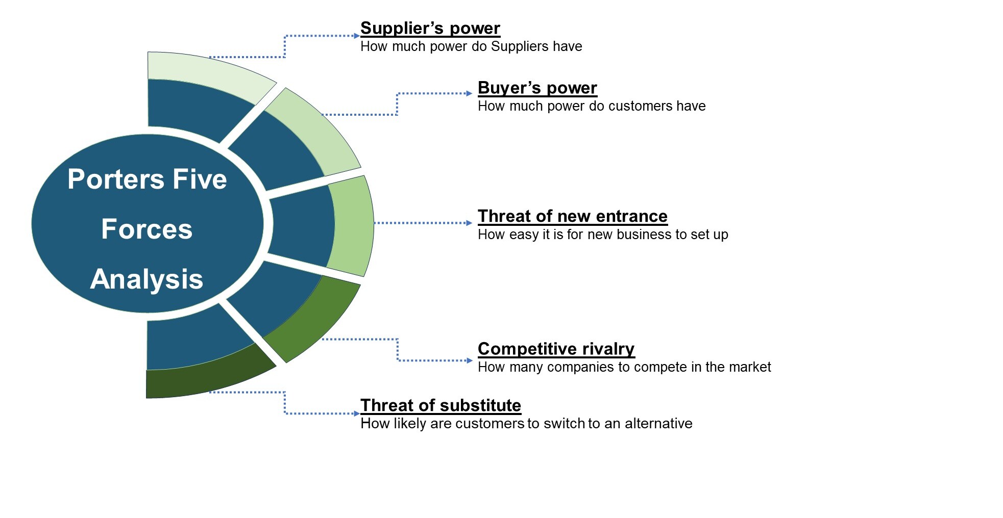
Porters Five Forces Analysis
We conduct Porter's Five Forces analysis to evaluate the competitive landscape of an industry, providing us with insights into factors that affect profitability and strategic positioning.
SWOT Analysis

Forecasting
We utilize a forecasting model to predict future consumption by considering parameters like population, economics, regulations, market competition, drivers, constraints, technology, and pricing. We also employ statistical techniques such as multilinear regression, exponential smoothing, moving average, ARIMA, and Monte Carlo simulations for accurate predictions. In econometric forecasting, we analyzed short-term and long-term event impacts, attributing values based on regulatory frameworks, economic factors, and market events.





 Speak to Our Analyst