Controlled Etch Market Size, Share, Trends and Growth Analysis, By Technology (Dry Etch [Plasma Etch], Wet Etch, and Atomic Layer Etch), By Process Type (Conductor Etch, Dielectric Etch, and Silicon Etch), By Application (Logic & Foundry, Memory, MEMS & Sensors, Advanced Packaging, and Other Applications), By End User (Foundries, IDMs, and OSATs), By Wafer Size (300mm, 200mm, and Other Wafer Sizes), and Region – Global Industry Report and Forecast, 2026–2035
Industry: Materials and Chemical | Publishing Date: August 5, 2026 | Last Updated: August 5, 2026 | No of Pages: N/A | No. of Tables: N/A | No. of Figures: N/A | Format: PDF | Report Code: MC5596
What Is the Controlled Etch Market Size?
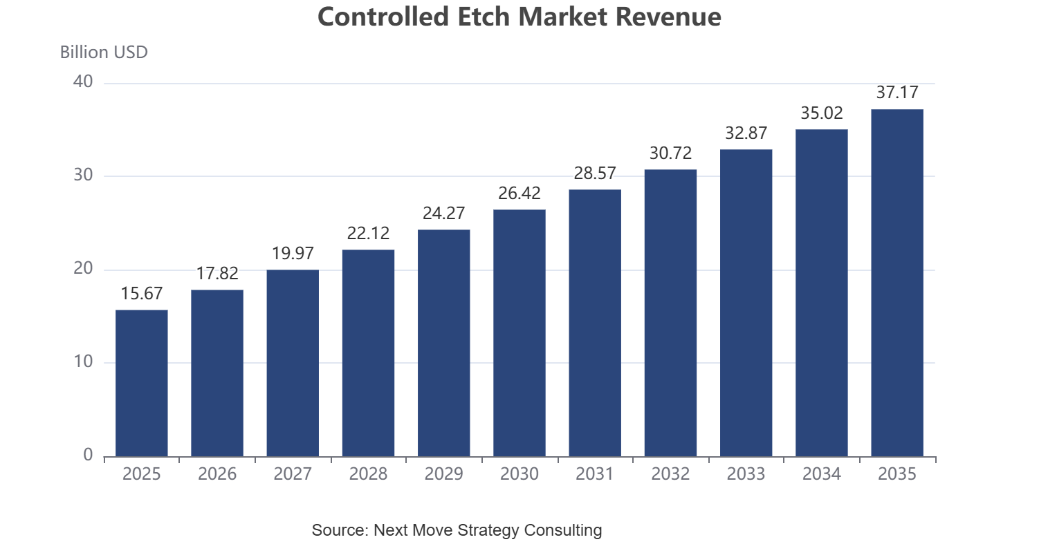
The global controlled etch market size was valued at USD 15.67 billion in 2025 and is estimated at USD 16.95 billion in 2026, forecast to reach USD 37.17 billion by 2035, expanding at a 9.10% CAGR between 2026 and 2035. Asia-Pacific leads with approximately 68% share, while dry etch systems dominate all other technologies with approximately 72% share.
We observed that growth is broad-based across every segmentation axis, with atomic layer etch adoption and advanced packaging applications driving the dominant structural shifts through 2035.
|
Key Takeaways |
|
By Technology: Dry Etch (Plasma Etch) held the largest share of approximately 72% (USD 11.28 Billion) in 2025; Atomic Layer Etch is the fastest-growing sub-segment at 16.1% CAGR from 2026–2035. |
|
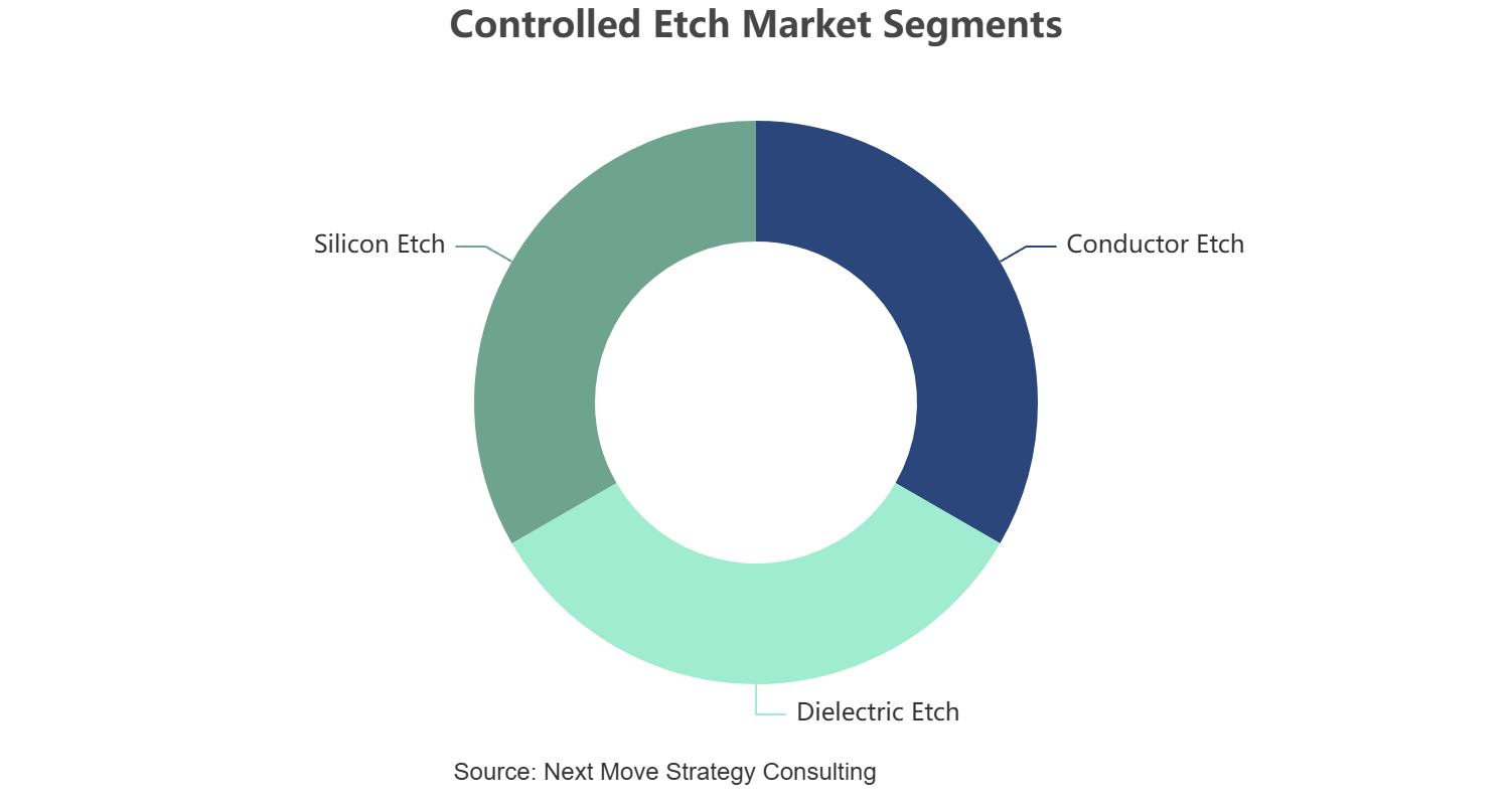
By Process Type: Conductor Etch held the largest share of approximately 38% (USD 5.95 Billion) in 2025; Dielectric Etch is the fastest-growing sub-segment at 9.8% CAGR from 2026–2035. |
|
By Application: Logic and Foundry held the largest share of approximately 41% (USD 6.42 Billion) in 2025; Advanced Packaging is the fastest-growing sub-segment at 14.1% CAGR from 2026–2035. |
|
By End User: Foundries held the largest share of approximately 46% (USD 7.21 Billion) in 2025; Outsourced Semiconductor Assembly and Test is the fastest-growing sub-segment at 12.1% CAGR from 2026–2035. |
|
By Wafer Size: 300mm held the largest share of approximately 79% (USD 12.38 Billion) in 2025; Other Wafer Sizes is the fastest-growing sub-segment at 11.1% CAGR from 2026–2035. |
|
Dominant Region: Asia-Pacific dominated with approximately 68% revenue share (USD 10.66 billion) in 2025. |
|
Fastest-Growing Region: Middle East & Africa is expected to register the highest CAGR of 12.1% during 2026–2035. |
|
Dominant Country: China led with approximately USD 3.09 billion in 2025. |
|
Fastest-Growing Country: India is the fastest-growing country at approximately 19.8% CAGR from 2026–2035. |
Market Opportunity: The controlled etch market is expected to create an absolute dollar opportunity of USD 20.22 billion between 2026 and 2035, presenting significant investment potential across the advanced semiconductor process equipment value chain.
According to Next Move Strategy Consulting analysis, foundries and memory manufacturers are increasingly specifying atomic-level plasma control and AI-enabled process sensors to manage yield at sub-3nm and advanced 3D NAND nodes, a shift that favors etch equipment vendors with integrated process control capability over conventional plasma platforms as node scaling and advanced packaging complexity accelerate through 2035.
What Does the Controlled Etch Market Encompass?
The controlled etch market encompasses precision dry, wet, and atomic layer etch equipment and process technologies used to selectively remove material from semiconductor wafers during fabrication. Our assessment indicates that the scope spans conductor, dielectric, and silicon etch processes deployed across logic, memory, and advanced packaging applications, forming a core segment of the broader semiconductor wafer fab equipment category supplied to foundries, integrated device manufacturers, and outsourced semiconductor assembly and test providers.
Regulatory frameworks such as export control restrictions on advanced semiconductor equipment increasingly shape cross-border sales and technology transfer within the industry. We observed that technology adoption is shifting toward atomic layer etch and AI-enabled plasma control systems that improve yield precision at advanced process nodes. Next Move Strategy Consulting's analysis indicates that this structural shift, combined with surging AI chip and high-performance computing demand, is redefining procurement criteria across the controlled etch market.
|
Field |
Details |
|
Market Size in 2025 |
USD 15.67 Billion |
|
Market Size in 2026 |
USD 16.95 Billion |
|
Revenue Forecast in 2035 |
USD 37.17 Billion |
|
Growth Rate |
CAGR of 9.10% from 2026 to 2035 |
|
Analysis Period |
2025–2035 |
|
Base Year Considered |
2025 |
|
Forecast Period |
2026–2035 |
|
Market Size Estimation |
USD Billion |
|
Companies Profiled |
12 |
|
Countries Covered |
33 |
|
Market Share |
Available for Top 10 Companies |
Key Emerging Trends
Based on research conducted by Next Move Strategy Consulting, we found that four structural trends are reshaping equipment design, fab adoption, and stakeholder engagement across the industry.
How Is AI-Enabled Plasma Control Transforming Conductor Etch Platforms?
AI-enabled plasma control is transforming conductor etch platforms as equipment vendors embed sensor-driven feedback loops to improve yield precision. We observed that Lam Research released its Akara conductor etch platform, combining atomic-level plasma control with artificial intelligence sensors for improved chip yield and wafer-level uniformity. Foundries and memory manufacturers are adopting similar AI-enabled etch systems to manage tightening process control requirements at advanced logic and 3D NAND nodes.
Why Is DRAM Capacity Expansion Driving Etch Equipment Investment?
DRAM capacity expansion is driving substantial etch equipment investment as memory manufacturers scale production to meet AI infrastructure demand. Our findings suggest that Tokyo Electron reportedly raised its fiscal year 2026 capital expenditure guidance by approximately 48% to a record high, citing rising DRAM etching demand. This trend is elevating demand for dielectric and conductor etch systems among memory-focused integrated device manufacturers expanding capacity for high-bandwidth memory production.
How Is Advanced Packaging Expansion Reshaping Etch Equipment Demand?
Advanced packaging expansion is reshaping etch equipment demand as chipmakers pursue heterogeneous integration to extend performance scaling beyond traditional transistor shrinkage. We observed that Lam Research is extending its core etch and deposition expertise into advanced packaging applications, following broader industry moves by equipment makers to serve chip-stacking and panel-level packaging processes. This trend is elevating demand for etch systems among outsourced semiconductor assembly and test providers pursuing next-generation packaging capability.
What Role Does Export Control Policy Play in Reshaping Regional Equipment Sales?
Export control policy continues to reshape regional equipment sales patterns as governments restrict advanced semiconductor equipment transfers to specific markets. Our analysis shows that equipment makers including Applied Materials and Lam Research have publicly addressed the impact of expanded export restrictions on China-bound sales, while some Japanese and Dutch equipment makers have secured partial servicing exemptions. This trend, while creating near-term revenue uncertainty, is elevating demand for equipment sales diversification across non-restricted markets.
Pestel Analysis of the Controlled Etch Market
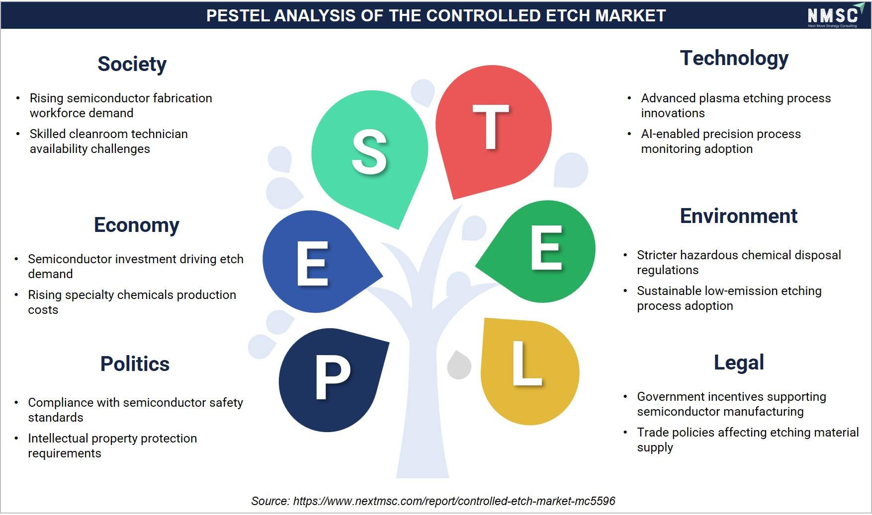
The PESTEL analysis of the market highlights the external factors influencing semiconductor manufacturing and precision fabrication. Political support for domestic chip production, economic investments in semiconductor capacity, and growing demand for advanced electronics drive market growth. Technological advancements in plasma and atomic layer etching improve process precision, while environmental regulations encourage sustainable chemical usage. Legal compliance with safety, quality, and environmental standards further supports innovation and global market competitiveness.
Growth Drivers and Restraints
Growth Catalyst and Risk Assessment Matrix
|
Factors |
Type |
(+/−) % Impact on CAGR |
Geographic Relevance |
Impact Timeline |
|
Rising AI chip and high-performance computing demand |
Driver |
+3.1% |
Global |
2026–2035 |
|
Expanding DRAM and 3D NAND memory capacity investment |
Driver |
+2.4% |
Asia-Pacific |
2026–2035 |
|
Growing advanced node logic and foundry capacity expansion |
Driver |
+1.9% |
Asia-Pacific, North America |
2026–2035 |
|
Rising advanced packaging and heterogeneous integration adoption |
Driver |
+1.4% |
Global |
2026–2032 |
|
Government semiconductor manufacturing incentive programmes |
Driver |
+1.1% |
North America, Europe, Asia-Pacific |
2026–2035 |
|
Expanding atomic layer etch adoption at sub-3nm nodes |
Driver |
+0.8% |
Global |
2026–2035 |
|
Export control restrictions limiting cross-border equipment sales |
Restraint |
−1.4% |
Asia-Pacific |
2026–2035 |
|
High capital cost of advanced etch systems limiting smaller fabs |
Restraint |
−0.9% |
Global |
2026–2032 |
|
Cyclical sensitivity of semiconductor capital expenditure to demand swings |
Restraint |
−0.6% |
Global |
2028–2035 |
What Is the Primary Growth Driver of the Controlled Etch Market?
Rising AI chip and high-performance computing demand is the primary driver of the market. Corporate financial disclosures from leading etch equipment vendors continue to cite AI semiconductor and high-performance computing demand as a primary driver of quarterly performance expectations. We observed that this AI-driven demand pace, reinforced by expanding foundry and memory capacity investment, continues to anchor baseline demand for conductor and dielectric etch systems across developed and emerging semiconductor manufacturing economies alike.
How Is DRAM Capacity Expansion Driving Controlled Etch Market Growth?
Expanding DRAM and 3D NAND memory capacity investment is accelerating market growth toward dielectric and conductor etch categories. Corporate capital expenditure guidance from major equipment vendors continues to disclose substantial year-over-year increases tied to memory manufacturer capacity expansion. Our assessment indicates that this capacity expansion pace, combined with rising high-bandwidth memory demand for AI infrastructure, is compressing adoption timelines for advanced etch systems across Asia-Pacific memory manufacturing hubs.
What Is Restraining Controlled Etch Market Expansion?
Export control restrictions limiting cross-border equipment sales restrain revenue growth among equipment vendors serving restricted markets. Corporate disclosures from major U.S. equipment makers continue to cite expanded export control measures as a factor affecting China-bound sales and service revenue. We found that equipment vendors diversifying sales toward non-restricted markets and expanding domestic manufacturing capacity in unrestricted regions are beginning to offset this restraint, though full mitigation remains gradual.
Segmentation Analysis
Segment Sizing: By Technology
|
Segment |
2025 (USD) |
2035 (USD) |
CAGR% (2026–2035) |
|
Dry Etch (Plasma Etch) |
USD 11.28 Billion |
USD 25.84 Billion |
8.7% |
|
Wet Etch |
USD 2.98 Billion |
USD 5.49 Billion |
6.1% |
|
Atomic Layer Etch |
USD 1.41 Billion |
USD 5.84 Billion |
16.1% |
|
Total |
USD 15.67 Billion |
USD 37.17 Billion |
9.1% |
Which Technology Segment Dominates the Controlled Etch Market?
Dry Etch (Plasma Etch) led the market with USD 11.28 billion in 2025, supported by its established role as the primary etch technology for high-precision conductor and dielectric patterning at advanced logic and memory nodes. We observed that Atomic Layer Etch is the fastest-growing technology, expanding at a 16.1% CAGR from 2026 to 2035, as sub-3nm node development and gate-all-around transistor architectures require atomic-scale material removal precision beyond conventional plasma etch capability.
Segment Sizing: By Application
|
Segment |
2025 (USD) |
2035 (USD) |
CAGR% (2026–2035) |
|
Logic and Foundry |
USD 6.42 Billion |
USD 14.90 Billion |
8.8% |
|
Memory |
USD 5.17 Billion |
USD 11.09 Billion |
7.9% |
|
MEMS and Sensors |
USD 1.72 Billion |
USD 4.08 Billion |
9.1% |
|
Advanced Packaging |
USD 1.57 Billion |
USD 5.56 Billion |
14.1% |
|
Other Applications |
USD 0.78 Billion |
USD 1.55 Billion |
6.9% |
|
Total |
USD 15.67 Billion |
USD 37.17 Billion |
9.1% |
Which Application Segment Leads Controlled Etch Market Demand?
Logic and Foundry remained the leading application, valued at USD 6.42 billion in 2025 as leading-edge foundries continue expanding advanced node production capacity for AI and high-performance computing chips. Based on research conducted by Next Move Strategy Consulting, we found that Advanced Packaging is the fastest-growing application at a 14.1% CAGR from 2026 to 2035, reflecting rising chip-stacking and heterogeneous integration adoption among leading semiconductor and packaging companies.
Segment Sizing: By End User
|
Segment |
2025 (USD) |
2035 (USD) |
CAGR% (2026–2035) |
|
Foundries |
USD 7.21 Billion |
USD 16.74 Billion |
8.9% |
|
Integrated Device Manufacturers |
USD 6.11 Billion |
USD 13.32 Billion |
8.1% |
|
Outsourced Semiconductor Assembly and Test |
USD 2.35 Billion |
USD 7.11 Billion |
12.1% |
|
Total |
USD 15.67 Billion |
USD 37.17 Billion |
9.1% |
Which End User Segment Leads Controlled Etch Adoption?
Foundries remained the dominant end user, reaching USD 7.21 billion in 2025 due to their concentrated capital expenditure on advanced node capacity serving fabless logic and AI chip designers. Our findings suggest that Outsourced Semiconductor Assembly and Test is the fastest-growing end user at a 12.1% CAGR from 2026 to 2035, reflecting expanding advanced packaging capacity investment among providers serving heterogeneous integration and chip-stacking demand.
Growth Opportunities
Our analysis shows that three forward-looking opportunities stand out for stakeholders positioning within the market over the 2026–2035 forecast period.
How Can Atomic Layer Etch Systems Unlock Value for Advanced Node Foundries?
Atomic layer etch systems present a whitespace opportunity for equipment vendors targeting foundries scaling gate-all-around and sub-3nm process nodes. Suppliers that scale precision ALE capability alongside AI-enabled process control stand to capture premium pricing as advanced logic manufacturers producing AI chips require atomic-scale material removal precision that conventional plasma etch systems cannot reliably deliver at next-generation process geometries.
Where Does Advanced Packaging Etch Create New Demand?
Chip-stacking and heterogeneous integration processes represent an underpenetrated opportunity for etch equipment vendors extending core semiconductor expertise into advanced packaging applications. Suppliers that adapt conductor and dielectric etch platforms for panel-level and wafer-level packaging can secure new outsourced semiconductor assembly and test customers, benefiting from rising demand for multi-die integration in AI accelerator and high-performance computing chip designs.
How Can Export-Compliant Manufacturing Benefit Equipment Vendors?
Equipment vendors navigating export control complexity create an opportunity through regionally diversified manufacturing and servicing capability. Early movers that establish export-compliant production and support infrastructure across multiple regions can differentiate with foundries and memory manufacturers pursuing supply chain resilience amid ongoing geopolitical uncertainty affecting cross-border semiconductor equipment transfers.
Supply Chain Structure of the Controlled Etch Market
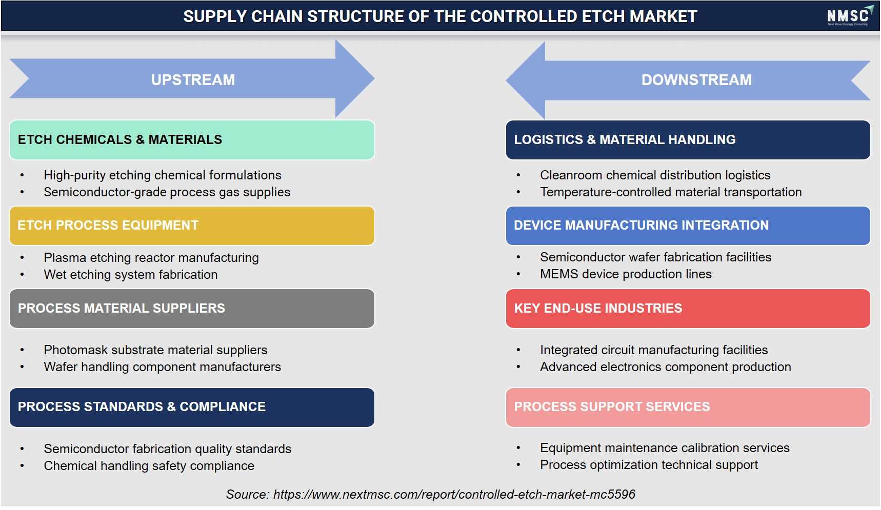
The market supply chain begins with high-purity etching chemicals, process gases, and specialized equipment used in semiconductor fabrication. Material suppliers provide photomasks, wafers, and critical process components, while compliance with semiconductor quality and chemical safety standards ensures reliable production. Downstream, temperature-controlled logistics and cleanroom handling support semiconductor manufacturing, MEMS production, and advanced electronics fabrication. Equipment maintenance, process optimization, and technical support services enhance operational efficiency and ensure consistent etching performance across manufacturing facilities.
Regional Outlook
Geographic Performance Snapshot
|
Region |
2025 (USD) |
2035 (USD) |
CAGR% (2026–2035) |
Key Driver |
|
Asia-Pacific |
USD 10.66 Billion |
USD 25.77 Billion |
9.4% |
Concentrated foundry and memory manufacturing capacity and dense equipment supply base |
|
North America |
USD 2.51 Billion |
USD 5.47 Billion |
8.1% |
Domestic semiconductor manufacturing incentive programmes and advanced fab investment |
|
Europe |
USD 1.57 Billion |
USD 3.33 Billion |
7.8% |
National semiconductor sovereignty initiatives and specialty fab investment |
|
Middle East & Africa |
USD 0.47 Billion |
USD 1.42 Billion |
12.1% |
Emerging semiconductor investment diversification and technology infrastructure programmes |
|
Latin America |
USD 0.47 Billion |
USD 1.18 Billion |
9.8% |
Growing electronics manufacturing investment and technology infrastructure expansion |
|
Total |
USD 15.67 Billion |
USD 37.17 Billion |
9.1% |
— |
North America Controlled Etch Market Outlook
North America's market reflects growing momentum supported by domestic semiconductor manufacturing incentive programmes and expanding advanced fab investment. We observed that leading equipment vendors headquartered in the region continue to disclose strong order backlogs tied to AI chip and high-performance computing demand. Technology adoption remains advanced, with atomic layer etch and AI-enabled plasma control systems expanding across the region's foundry and advanced packaging sectors.
Europe Controlled Etch Market Outlook
Europe's controlled etch market reflects a specialized landscape shaped by national semiconductor sovereignty initiatives and targeted fab investment programmes. Our findings suggest that manufacturers across Germany, France, and the UK are accelerating adoption of advanced etch systems to support specialty semiconductor and automotive chip production. Technology adoption favors established dry etch platforms, supported by regional fabs investing in capacity modernization.
Asia-Pacific Controlled Etch Market Outlook
Asia-Pacific leads the controlled etch market with the most concentrated foundry and memory manufacturing capacity globally, anchored by leading fabs in China, Japan, and South Korea. We found that regulatory frameworks, including export control measures, meaningfully shape equipment sourcing decisions across the region. Technology adoption is accelerating as regional manufacturers, including several China-based equipment makers, expand production capacity to serve growing domestic demand.
Middle East & Africa Controlled Etch Market Outlook
The controlled etch market in Middle East & Africa is the fastest-growing region as Gulf Cooperation Council economies invest in semiconductor and technology infrastructure diversification programmes. Our analysis shows that Saudi Arabia and the UAE are attracting early-stage semiconductor investment tied to Vision 2030-linked technology diversification. Regulatory influence remains moderate, while technology adoption is gradually emerging as regional governments pursue technology sector development.
Latin America Controlled Etch Market Outlook
Latin America's controlled etch market is supported by growing electronics manufacturing investment in Brazil and Argentina and expanding technology infrastructure programmes. We observed that regulatory frameworks are less developed than in North America or Asia-Pacific, though the region's electronics assembly base is gradually attracting complementary semiconductor process investment. Technology adoption remains nascent, with competitive intensity increasing as global equipment vendors explore regional support partnerships.
U.S. Controlled Etch Market
Based on our estimates, the U.S. market was valued at approximately USD 2.21 billion in 2025, projected to reach USD 4.81 billion by 2035 at a 8.1% CAGR. Demand structure is anchored by strong domestic semiconductor manufacturing incentive programmes and leading etch equipment vendor headquarters. Technology penetration favors AI-enabled and atomic layer etch systems, and competitive intensity remains high among established U.S.-headquartered equipment makers serving national and export foundry accounts.
Canada Controlled Etch Market
The market in Canada was valued at approximately USD 0.15 billion in 2025 and is projected to reach USD 0.30 billion by 2035, growing at a 7.1% CAGR. Demand is reflecting demand patterns tied to specialty semiconductor and electronics manufacturing investment. Technology penetration is rising as fabs request advanced etch systems, with competitive intensity moderate given reliance on cross-border equipment supply from U.S.-based vendors.
UK Controlled Etch Market
As per our estimate, the UK market was valued at approximately USD 0.17 billion in 2025, projected to reach USD 0.34 billion by 2035 at a 6.9% CAGR. Demand structure is driven by specialty semiconductor fab investment and growing compound semiconductor manufacturing activity. Regulatory influence from UK technology sovereignty initiatives is emerging, technology penetration favors established dry etch platforms, and competitive intensity remains steady among European and global equipment vendors.
Germany Controlled Etch Market
According to our analysis, the Germany market was valued at approximately USD 0.53 billion in 2025, projected to reach USD 1.16 billion by 2035 at a 8.1% CAGR. Demand structure is benefiting from a strong domestic automotive and specialty semiconductor manufacturing base pursuing capacity expansion under national semiconductor strategy. Germany's technology sovereignty initiatives drive regulatory influence, while technology penetration favors advanced dielectric and conductor etch systems among leading specialty fabs.
France Controlled Etch Market
Based on our estimates, the France market was valued at approximately USD 0.25 billion in 2025, projected to reach USD 0.48 billion by 2035 at a 6.6% CAGR. Demand structure is supported by France's growing semiconductor manufacturing investment and specialty fab expansion. Regulatory influence from French and EU semiconductor sovereignty frameworks is notable, and competitive intensity remains moderate given the concentration of specialty fabs serving automotive and industrial applications.
China Controlled Etch Market
The market in China was valued at approximately USD 3.09 billion in 2025 and is projected to reach USD 9.34 billion by 2035, growing at a 12.1% CAGR. Demand is fueled by substantial domestic foundry and memory capacity expansion and a dense base of regional equipment suppliers. Regulatory influence is significant given export control measures affecting equipment sourcing, technology penetration is accelerating through domestic equipment maker capacity expansion, and competitive intensity remains elevated among numerous China-based manufacturers.
India Controlled Etch Market
As per our estimate, the India market was valued at approximately USD 0.43 billion in 2025, projected to reach USD 2.34 billion by 2035 at a 19.8% CAGR. Demand structure is the fastest among covered countries, reflecting rapid semiconductor fab investment growth under national semiconductor mission programmes. Regulatory influence remains developing, while technology penetration is rising quickly as multinational equipment vendors establish support infrastructure to serve India's emerging fab ecosystem.
Japan Controlled Etch Market
According to our analysis, the Japan market was valued at approximately USD 2.34 billion in 2025, projected to reach USD 4.70 billion by 2035 at a 7.1% CAGR. Demand structure is supported by Japan's deep semiconductor equipment manufacturing heritage and leading domestic equipment vendor headquarters. Regulatory influence is well established, technology penetration is advanced, and competitive intensity remains high among long-standing domestic and global equipment makers.
South Korea Controlled Etch Market
Based on our estimates, the South Korea market was valued at approximately USD 2.56 billion in 2025, projected to reach USD 5.81 billion by 2035 at a 8.6% CAGR. Demand structure is benefiting from the country's globally dominant memory manufacturing base and substantial DRAM and NAND capacity investment. Technology penetration is high, with leading memory manufacturers driving advanced etch system adoption, and competitive intensity remains pronounced amid rapid capacity expansion cycles.
Australia Controlled Etch Market
The market in Australia was valued at approximately USD 0.11 billion in 2025 and is projected to reach USD 0.20 billion by 2035, growing at a 6.1% CAGR. Demand is supported by emerging technology sector investment and growing interest in semiconductor supply chain diversification. Regulatory influence stems from Australia's technology security frameworks, while technology penetration favors imported standard etch systems amid limited domestic fab capacity.
UAE Controlled Etch Market
As per our estimate, the UAE market was valued at approximately USD 0.15 billion in 2025, projected to reach USD 0.48 billion by 2035 at a 13.1% CAGR. Demand structure is shaped by the UAE's role as an emerging regional technology investment hub pursuing semiconductor sector diversification. Regulatory influence remains moderate, technology penetration is improving through early-stage technology infrastructure investment, and competitive intensity is rising as vendors explore regional partnerships.
Saudi Arabia Controlled Etch Market
According to our analysis, the Saudi Arabia market was valued at approximately USD 0.14 billion in 2025, projected to reach USD 0.47 billion by 2035 at a 13.8% CAGR. Demand structure is driven by Vision 2030-linked technology diversification and emerging semiconductor sector investment interest. Regulatory influence is developing under national technology strategy guidelines, and technology penetration is advancing as the country pursues early-stage semiconductor ecosystem development.
South Africa Controlled Etch Market
Based on our estimates, the South Africa market was valued at approximately USD 0.06 billion in 2025, projected to reach USD 0.14 billion by 2035 at a 9.8% CAGR. Demand structure is reflecting nascent semiconductor and electronics manufacturing interest within the broader regional technology sector. Regulatory influence is limited, technology penetration remains early-stage, and competitive intensity is low given minimal domestic fab capacity.
Brazil Controlled Etch Market
The market in Brazil was valued at approximately USD 0.22 billion in 2025 and is projected to reach USD 0.57 billion by 2035, growing at a 10.1% CAGR. Demand is supported by growing electronics manufacturing investment and gradual technology infrastructure expansion. We observed that regulatory frameworks remain less developed than in North America or Asia-Pacific, though the region's electronics assembly base is attracting complementary process investment across major metropolitan markets.
Argentina Controlled Etch Market
As per our estimate, the Argentina market was valued at approximately USD 0.07 billion in 2025, projected to reach USD 0.16 billion by 2035 at a 8.8% CAGR. Demand structure is reflecting early-stage technology infrastructure investment amid gradual electronics manufacturing sector growth. Regulatory influence remains limited, technology penetration is nascent, and competitive intensity is low among regional distributors serving emerging technology accounts.
Competitive Landscape
We observed that the controlled etch market remains highly consolidated among a small group of established semiconductor process equipment vendors, with Japanese and U.S. manufacturers holding the deepest technology leadership.
|
Field |
Details |
|
Market Structure |
Highly consolidated, led by a small group of established U.S. and Japanese equipment vendors |
|
Innovation Focus |
AI-enabled plasma control, atomic layer etch precision, and advanced packaging extension |
|
M&A Activity |
Selective, concentrated in advanced packaging capability acquisition and regional expansion |
How Do Companies Compete in the Controlled Etch Market?
Companies compete primarily on process precision, AI-enabled control capability, and customer relationships with leading foundries and memory manufacturers across the industry. Established vendors such as Lam Research Corporation and Applied Materials, Inc. leverage deep process engineering and long-standing fab relationships, while Tokyo Electron Limited competes on Asia-Pacific manufacturing proximity and integrated equipment platform breadth serving regional memory and logic customers.
Which Competitive Archetypes Dominate the Controlled Etch Market?
Two archetypes dominate the market: diversified U.S. equipment vendors offering integrated etch, deposition, and packaging platforms, and Japanese and Asian equipment makers focused on precision process engineering and regional manufacturing proximity. Lam Research Corporation and Applied Materials, Inc. exemplify the diversified U.S. archetype through broad platform portfolios, while Tokyo Electron Limited and SCREEN Holdings Co., Ltd. exemplify the Japanese archetype through deep process precision and Asia-Pacific customer proximity.
How Are Companies Differentiating Through Innovation in Controlled Etch?
Innovation and differentiation strategy increasingly center on AI-enabled process control and atomic-scale precision. Lam Research's Akara conductor etch platform, combining atomic-level plasma control with AI sensors for improved yield, exemplifies how vendors are embedding machine learning directly into process equipment. Our analysis shows that equipment makers unable to demonstrate AI-enabled yield improvement risk losing advanced node contracts to competitors with validated precision control capability.
What M&A and Expansion Activity Is Shaping the Controlled Etch Market?
Capability extension into advanced packaging and capacity expansion continue to shape competitive positioning within the industry. Lam Research's extension of core etch and deposition expertise into advanced packaging applications, alongside Tokyo Electron's reported 48% capital expenditure increase tied to rising DRAM etching demand, illustrates how leading vendors are simultaneously expanding into new application areas and scaling production capacity to meet AI-driven semiconductor demand.
Key Market Players
Our assessment indicates that the following 12 companies are actively shaping process innovation, manufacturing capacity, and commercial strategy within the global controlled etch market.
-
Applied Materials, Inc.
-
Lam Research Corporation
-
Tokyo Electron Limited
-
Hitachi High-Tech Corporation
-
Oxford Instruments plc
-
SCREEN Holdings Co., Ltd.
-
Panasonic Corporation
-
SEMES Co., Ltd.
-
NAURA Technology Group Co., Ltd.
-
Advanced Micro-Fabrication Equipment Inc. China
-
Plasma-Therm LLC
-
ULVAC, Inc.
Latest Developments
We found that recent activity within the controlled etch market is concentrated on AI-enabled platform launches and capital expenditure expansion, reflecting the industry's response to surging AI chip and memory demand.
|
Date |
Event |
|
June 2026 |
Applied Materials introduced the Producer Selectra Mo Etch system, a selective metal etch platform for advanced 3D NAND manufacturing. The new system enables highly selective molybdenum removal with precise and uniform wordline separation, overcoming the limitations of conventional wet etching through engineered process control and advanced gas delivery. The technology improves manufacturing yield, reduces cell-to-cell variability, and enables continued scaling of next-generation 3D NAND devices. |
|
February 2025 |
Lam Research launched the Akara conductor etch platform, its most advanced plasma etch system to date. The system incorporates DirectDrive® solid-state plasma technology, enabling plasma response more than 100× faster than previous systems, delivering atomic-scale precision for advanced 3D semiconductor manufacturing. This launch strengthens Lam's position in the controlled etch equipment market for logic and memory chips. |
Investment Opportunities
What Capital Inflows Are Targeting the Controlled Etch Market?
Capital inflows into the controlled etch market are increasingly directed toward AI-enabled process control and advanced packaging capability. Corporate capital expenditure guidance from leading equipment vendors continues to disclose substantial increases tied to memory and advanced node demand. We observed that investors favor equipment makers demonstrating validated AI-enabled yield improvement, viewing process control innovation as a proxy for long-term foundry and memory manufacturer contract retention.
How Is Infrastructure Investment Supporting Controlled Etch Market Growth?
Infrastructure investment is expanding equipment manufacturing capacity and regional support infrastructure to meet surging AI chip and memory demand. Our findings suggest that Tokyo Electron's reported 48% capital expenditure increase illustrates the scale of investment required to keep pace with DRAM and advanced node etching equipment demand, reinforcing how equipment vendors are prioritizing capacity expansion alongside continued process innovation.
What ESG Considerations Are Shaping Controlled Etch Investment Decisions?
Environmental, social, and governance considerations are increasingly relevant to investment decisions across the industry, with process gas emissions reduction and energy-efficient equipment design as key criteria. Corporate sustainability disclosures from major equipment vendors continue to report process efficiency improvements alongside capital expenditure figures. We found that investors increasingly favor equipment makers with validated energy efficiency and emissions reduction credentials, treating sustainable process design as a governance indicator alongside export compliance practices.
Key Benefits for Stakeholders
How Does This Report Benefit Enterprise and Industry Leaders?
Enterprise and industry leaders gain access to validated segmentation, competitive benchmarking, and regional demand forecasts that support sourcing and capital investment decisions across the controlled etch industry. Our analysis shows that detailed technology, application, and end user breakdowns help procurement teams align equipment investment with process node requirements while identifying underserved segments for expansion.
How Does This Report Benefit Investors and Financial Analysts?
Investors and financial analysts benefit from consistent, single-point market size and CAGR estimates that support valuation and capital-allocation decisions across the controlled etch market supply chain. We observed that the report's regional and segment-level growth differentials help identify which equipment vendors are best positioned to capture above-market growth in atomic layer etch and advanced packaging categories through 2035.
How Does This Report Benefit Technology Vendors and Product Teams?
Technology vendors and product teams gain insight into emerging design requirements, including AI-enabled plasma control, atomic layer precision, and advanced packaging capability, that are reshaping the industry. Our findings suggest that this analysis helps R&D teams prioritize development roadmaps around yield-improving process control and export-compliant manufacturing that are increasingly required by foundry and memory manufacturer procurement processes.
Key Market Segments
By Technology
-
Dry Etch (Plasma Etch)
-
Wet Etch
-
Atomic Layer Etch
By Process Type
-
Conductor Etch
-
Dielectric Etch
-
Silicon Etch
By Application
-
Logic and Foundry
-
Memory
-
MEMS and Sensors
-
Advanced Packaging
-
Other Applications
By End User
-
Foundries
-
Integrated Device Manufacturers
-
Outsourced Semiconductor Assembly and Test
By Wafer Size
-
300mm
-
200mm
-
Other Wafer Sizes
By Region
-
North America: U.S., Canada, Mexico
-
Europe: UK, Germany, France, Italy, Spain, Sweden, Denmark, Finland, Netherlands, Rest of Europe
-
Asia-Pacific: China, India, Japan, South Korea, Taiwan, Indonesia, Vietnam```html , Australia, Philippines, Malaysia, Rest of APAC
-
Middle East & Africa: Saudi Arabia, UAE, Egypt, Israel, Turkey, Nigeria, South Africa, Rest of MEA
-
Latin America: Brazil, Argentina, Chile, Colombia, Rest of LATAM
Conclusion and Recommendations
What Is the Long-Term Outlook for the Controlled Etch Market?
The long-term outlook for the market remains positive, with global revenue projected to more than double from USD 15.67 billion in 2025 to USD 37.17 billion by 2035 at a 9.10% CAGR. We observed that sustained AI chip demand, expanding memory capacity investment, and rising advanced packaging adoption will continue underpinning demand across logic, memory, and packaging applications through the forecast period.
What Strategic Positioning Should Controlled Etch Suppliers Pursue?
Suppliers should prioritize AI-enabled process control and atomic layer etch capability while pursuing advanced packaging platform extension to secure long-term foundry and memory manufacturer contracts. Our assessment indicates that equipment vendors investing early in export-compliant regional manufacturing and precision yield technology will be best positioned to capture premium pricing within the controlled etch market.
How Attractive Is the Controlled Etch Market for New Investment?
The controlled etch industry presents an attractive investment case, supported by a USD 20.22 billion absolute dollar opportunity between 2026 and 2035 and above-average growth in atomic layer etch and advanced packaging categories. We found that investment attractiveness is highest for equipment vendors combining validated AI-enabled precision control with diversified regional manufacturing capability, positioning them to serve both leading-edge and export-restricted market segments simultaneously.
What Market Shifts and Key Risks Should Stakeholders Monitor?
Stakeholders should monitor export control policy changes, semiconductor capital expenditure cyclicality, and high equipment capital costs as key risks to the controlled etch market. Our analysis shows that equipment vendors unable to navigate export restrictions risk losing access to major Asia-Pacific customer bases, particularly within China's increasingly restriction-sensitive procurement environment.
What Are the Key Growth Pathways for the Controlled Etch Market?
Key growth pathways include expanding atomic layer etch adoption, scaling advanced packaging platform capability, and deepening penetration into outsourced semiconductor assembly and test end user accounts. Next Move Strategy Consulting's analysis indicates that suppliers pursuing these pathways while maintaining export compliance discipline will be best positioned to capture the controlled etch market's projected growth through 2035.
About the Author
 Liza Phukan
— Liza Phukan is Research Associate at Next Move Strategy Consulting, where she has covered emerging industries and market research across sectors for 3.5 years. Her work includes analyzing industry developments, validating market data, and developing structured business content from research findings. She uses secondary research and data-validation practices to turn complex market information into clear decision-useful market analysis for business audiences and support report development and B2B.
Liza Phukan
— Liza Phukan is Research Associate at Next Move Strategy Consulting, where she has covered emerging industries and market research across sectors for 3.5 years. Her work includes analyzing industry developments, validating market data, and developing structured business content from research findings. She uses secondary research and data-validation practices to turn complex market information into clear decision-useful market analysis for business audiences and support report development and B2B.
About the Reviewer
 Supradip Baul
— Supradip Baul is an accomplished business consultant and strategist with over a decade of rich experience in market intelligence, strategy, technology, and business transformation. His work has included rigorous qualitative and quantitative analysis across multiple industries, helping clients shape investment decisions and long-term roadmaps. Earlier in his career, he was associated with Gartner, where he contributed to industry-leading reports and market share analyses. He has worked with leading global companies and holds an MBA with a dual specialization in Marketing and Finance.
Supradip Baul
— Supradip Baul is an accomplished business consultant and strategist with over a decade of rich experience in market intelligence, strategy, technology, and business transformation. His work has included rigorous qualitative and quantitative analysis across multiple industries, helping clients shape investment decisions and long-term roadmaps. Earlier in his career, he was associated with Gartner, where he contributed to industry-leading reports and market share analyses. He has worked with leading global companies and holds an MBA with a dual specialization in Marketing and Finance.
At Next Move Strategy Consulting, we understand that insightful market research is the cornerstone of successful business decisions. That's why we employ a robust and multifaceted approach, combining various methodologies to deliver the most accurate and actionable data for our clients.

Research Landscape
We navigate the world of research with two primary approaches:
Qualitative Approach
Our qualitative research methodologies involve immersive techniques such as in-depth interviews, focus groups, and observational studies. By engaging directly with individuals and stakeholders, we uncover valuable insights that quantitative data alone may overlook.

Quantitative Research
In tandem with qualitative methodologies, NMSC leverages the power of Quantitative Research to provide a robust foundation of numerical insights. Through systematic data collection and analysis, we quantify patterns, preferences, and market trends, offering a comprehensive view of the business landscape.
Our quantitative research approach employs diverse tools, including surveys, experiments, and statistical modelling. These methodologies enable us to gather data from a large and representative sample, ensuring the statistical significance of our findings. By employing structured questionnaires and standardized data collection methods, we guarantee the reliability and validity of the information we present to our clients.
Quantitative research is particularly effective in measuring the prevalence of trends, assessing market size, and gauging the impact of various factors on consumer behavior. The numerical precision attained through this approach equips our clients with actionable insights, facilitating data-driven decision-making and strategy formulation.


Our Specialized Toolbox for Industry-Specific Market Research
We deploy a specialized arsenal of techniques tailored to meet your unique requirements. Here's a glimpse into our comprehensive toolbox:

Information Procurement
The stage entails acquiring market data or relevant information through various sources and methodologies.


Market Research Approach
We utilize both top-down and bottom-up approaches in market research analysis to achieve a comprehensive understanding of the market dynamics, leveraging the broad perspective of industry trends and macroeconomic factors alongside detailed insights from specific segments and individual companies.

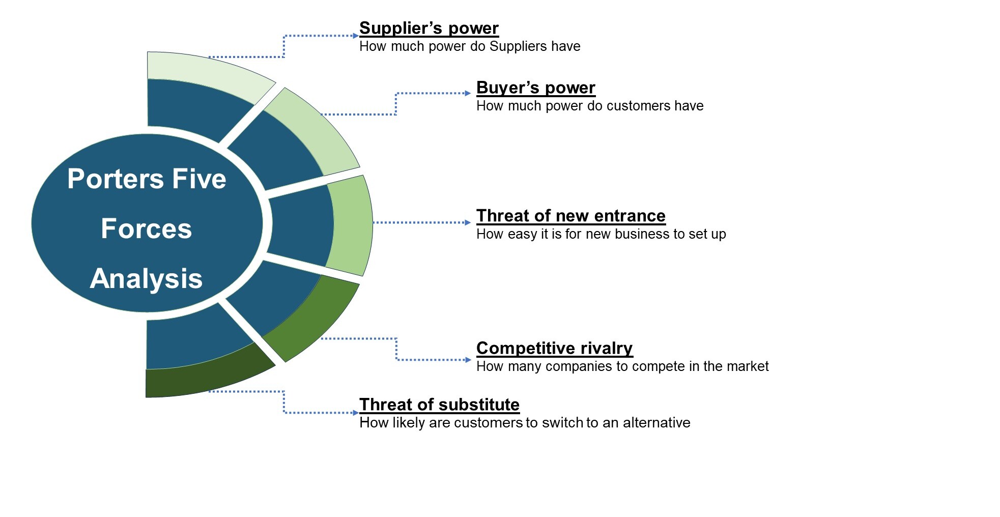
Porters Five Forces Analysis
We conduct Porter's Five Forces analysis to evaluate the competitive landscape of an industry, providing us with insights into factors that affect profitability and strategic positioning.
SWOT Analysis

Forecasting
We utilize a forecasting model to predict future consumption by considering parameters like population, economics, regulations, market competition, drivers, constraints, technology, and pricing. We also employ statistical techniques such as multilinear regression, exponential smoothing, moving average, ARIMA, and Monte Carlo simulations for accurate predictions. In econometric forecasting, we analyzed short-term and long-term event impacts, attributing values based on regulatory frameworks, economic factors, and market events.





 Speak to Our Analyst