How Are Nanochips Reshaping the Future of AI and Semiconductor Technology?

Artificial intelligence is evolving at a pace that is placing unprecedented pressure on global computing infrastructure. From data centers to cloud-based AI applications, the demand for faster and more energy-efficient processing systems continues to grow. At the center of this technological shift is the emergence of nanochips, particularly nanophotonic AI chips and advanced nanomanufacturing technologies.
The expanding Nanochip Market is gaining momentum as industries increasingly prioritize high-performance, low-energy semiconductor solutions capable of supporting next-generation AI workloads.
Recent developments from researchers at Sydney Nano Hub and Northeastern University are drawing attention because they address two major industry concerns simultaneously: rising energy consumption and the high cost of semiconductor manufacturing.
Why Are Nanochips Becoming Important for AI Development?
Traditional semiconductor chips rely on electrical signals moving through extremely dense nanoscale wiring systems. While this method has powered decades of computing progress, it also generates significant heat and requires extensive cooling infrastructure. As AI workloads become increasingly complex, these limitations are becoming more visible.
According to reporting published by Digital Journal, researchers at Sydney Nano Hub developed a nanochip that processes information using photons instead of electricity.
This form of photonic computing differs substantially from traditional electronic chip architecture. Instead of depending heavily on electrical conductivity, the system uses light particles to transfer and process information. Researchers believe this approach could reduce energy losses associated with conventional semiconductor systems.
The report also highlighted that photonic computing may integrate more smoothly with existing computing infrastructure than many earlier experimental technologies. This is particularly important because companies adopting new semiconductor solutions often face major compatibility and transition challenges.

How Could Nanophotonic Chips Improve Energy Efficiency?
One of the biggest operational concerns surrounding AI infrastructure is the enormous amount of heat generated during processing. Data centers already require sophisticated cooling systems that consume large amounts of electricity and water resources.
The Digital Journal report emphasized that heat and water usage are among AI’s most significant infrastructure vulnerabilities. Because nanophotonic chips rely less on electrical conductivity, researchers suggest they may generate lower levels of heat compared to conventional semiconductor systems.
Lower heat production could create several operational advantages. Cooling systems may require less energy, hardware components may experience reduced wear, and overall system efficiency could improve. These benefits are becoming increasingly important as AI applications continue expanding across industries.
The article also pointed to processing speed as another major advantage. Since photonic systems transfer information through light rather than electrical pathways, computing operations may become significantly faster. This could improve everything from enterprise AI processing to consumer-level applications such as gaming and advanced software systems.
|
Feature |
Conventional Chips |
Nanophotonic Chips |
|
Processing Method |
Electrical signals |
Photonic signals |
|
Heat Generation |
High |
Potentially lower |
|
Cooling Demand |
Extensive |
Potentially reduced |
|
Energy Efficiency |
Limited by conductivity |
Improved efficiency potential |
|
Processing Speed |
Conventional |
Faster optical transfer |
How Is Nanomanufacturing Changing Chip Production?

While improving semiconductor performance is important, manufacturing efficiency remains another major challenge for the industry.
According to Busnaina, traditional chip fabrication methods involve depositing layers of material and then removing excess material through etching processes. This approach requires expensive facilities, high temperatures, vacuum systems, and significant operational resources.
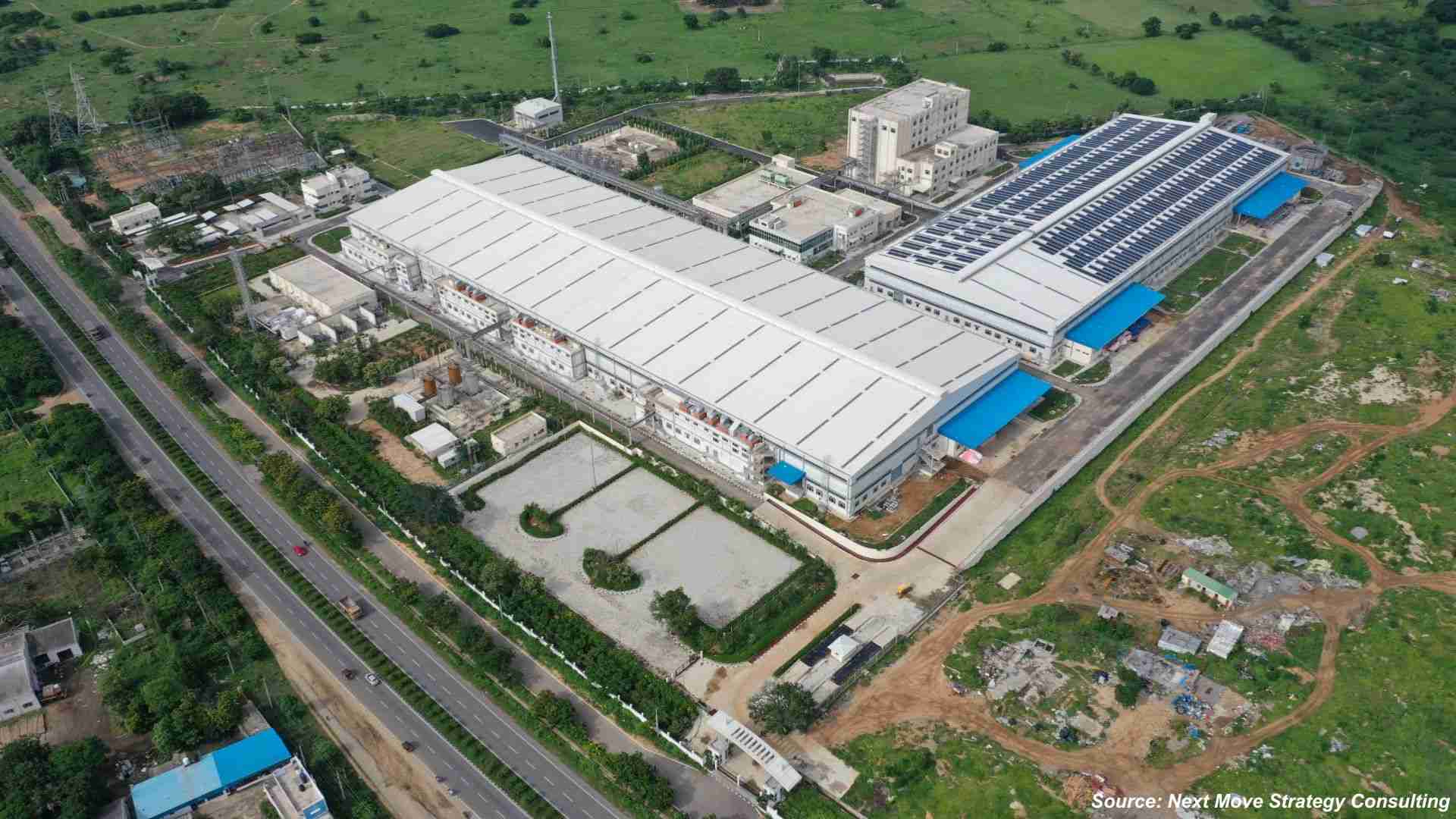
The report stated that advanced semiconductor fabrication facilities currently cost between $20 billion and $40 billion to build, while annual operating costs can reach approximately $1 billion. Additionally, a typical fabrication plant may consume an amount of electricity equivalent to 50,000 homes.
Busnaina’s patented process was developed to create a simpler and more affordable manufacturing alternative. The research aims to “democratize” microelectronics manufacturing by reducing barriers associated with cost, complexity, and production timelines.
Another major issue identified in the report is industry concentration. Due to the extreme costs involved in semiconductor fabrication, the number of companies capable of producing advanced chips reportedly declined from about 29 companies at the beginning of the millennium to only five companies by 2018.
Researchers believe that scalable nanomanufacturing systems may eventually help broaden participation in semiconductor innovation while reducing production inefficiencies.
|
Manufacturing Factor |
Conventional Fabrication |
|
Facility Construction Cost |
$20–40 billion |
|
Annual Operating Cost |
Around $1 billion |
|
Revision Timeline |
6 months–1 year |
|
Energy Requirement |
Equivalent to 50,000 homes |
How iSIM Technology Enhances Nanochip Integration
The image highlights the technological evolution from nano SIM to eSIM and finally to iSIM (integrated SIM) technology. It compares these SIM formats across several parameters, including size, security, cost efficiency, remote control capabilities, multiple profile support, and compatibility with Internet of Things (IoT) devices.
The diagram illustrates that iSIM technology integrates SIM functionality directly into the processor or system-on-chip architecture, eliminating the need for separate physical SIM hardware. Compared to traditional nano SIM and eSIM technologies, iSIM offers enhanced miniaturization, improved security integration, and greater efficiency for connected devices.
The visual also demonstrates how nanochip innovation is supporting compact semiconductor designs that are increasingly important for AI systems, IoT infrastructure, and next-generation smart devices.

Leading Companies Operating in the Nanochip Market
The Nanochip Market features the presence of several established semiconductor manufacturers and foundry service providers focused on advancing chip efficiency, nanomanufacturing capabilities, and next-generation AI processing technologies. Major companies operating in the industry include Taiwan Semiconductor Manufacturing Company Limited, Tower Semiconductor Ltd., Intel Corporation, Samsung Electronics, DB HiTek Co., Ltd., Hua Hong Semiconductor, Micron Technology, Inc., SK Hynix Inc., Rapidus Corporation, GlobalFoundries, Semiconductor Manufacturing International Corporation, United Microelectronics Corp., Texas Instruments, STMicroelectronics, and Advanced Micro Foundry. These companies are increasingly investing in advanced semiconductor fabrication technologies, energy-efficient chip architectures, and nanoscale manufacturing innovations to strengthen their competitive position in the evolving AI and semiconductor landscape.

What Major Trends Are Influencing Nanochip Innovation?
The latest developments suggest that nanochip research is no longer focused solely on processing power. Sustainability, manufacturing accessibility, and infrastructure efficiency are becoming equally important priorities.
AI expansion is increasing pressure on semiconductor developers to create systems that consume less energy while maintaining high-speed performance. At the same time, manufacturing costs are encouraging researchers to explore alternative production methods that reduce dependence on ultra-expensive fabrication facilities.
Photonic computing is also gaining momentum because it may integrate with existing infrastructure more effectively than some earlier experimental technologies. This compatibility could simplify adoption for enterprises investing heavily in AI infrastructure.
Next Steps for the Industry
Organizations investing in AI infrastructure may benefit from closely monitoring advancements in photonic semiconductor systems and scalable nanomanufacturing technologies. Semiconductor manufacturers are also likely to increase investments in lower-energy chip architectures as sustainability becomes a larger operational priority.
-
Invest in research focused on photonic computing and low-energy semiconductor systems.
-
Monitor developments in nanomanufacturing technologies that reduce fabrication costs.
-
Evaluate AI infrastructure upgrades that support energy-efficient chip integration.
-
Encourage collaboration between universities, semiconductor firms, and technology companies.
-
Prioritize sustainable chip production methods to reduce long-term operational costs.
Final Thoughts
Nanochips are emerging as one of the most promising developments in modern semiconductor research. Innovations from Sydney Nano Hub and Northeastern University demonstrate how photonic computing and advanced nanomanufacturing could address some of the industry’s most pressing challenges.
Although these technologies are still evolving, current research suggests that future semiconductor systems may become faster, more energy efficient, and more affordable to manufacture. As AI infrastructure continues expanding globally, nanochip innovation may play a central role in shaping the next generation of computing systems.
About the Author
 Tania Dey is a content writer specializing in transformation-led, insight-driven storytelling. She develops research-backed, high-impact content aligned with evolving business priorities, digital behavior, and audience expectations. Her work helps organizations sharpen value propositions, strengthen visibility, and communicate strategic intent with clarity and precision. Grounded in data-informed storytelling, she brings a strong focus on relevance, consistency, and measurable digital impact across platforms.
About the Reviewer
 Debashree Dey is a senior content writer and communications specialist known for crafting audience-focused narratives and insight-driven content strategies. As a published manuscript author, she combines creative storytelling with strategic thinking to strengthen brand messaging, enhance visibility, and drive meaningful audience engagement across digital platforms. With a collaborative leadership approach, she contributes to high-impact communication initiatives that ensure consistency, clarity, and long-term brand value. Outside of work, she finds inspiration in creative projects, design exploration, and storytelling-driven ideas.


Add Comment