Semiconductor Packing Market by Type (Embedded Die, Flip-Chip, Fan-In WLP, Fan-Out WLP), Packaging Material (Organic Substrate, Lead frame, Bonding Wire, Ceramic Package, Die Attach Material, and Others), Wafer Material (Simple Semiconductor, and Compound Semiconductor), Technology (Grid Array, Small Outline Package, Flat No-Leads Packages, Dual In-Line Package, and Others), and Others - Global Opportunity Analysis and Industry Forecast 2024-2030
Market Definition
The Semiconductor Packing Market size was valued at USD 34.59 billion in 2023 and is predicted to reach USD 64.22 billion by 2030 with a CAGR of 9.3% from 2024-2030. Semiconductor packaging refers to the process of enclosing or encapsulating a semiconductor device or integrated circuit (IC) in a protective package that provides electrical connections to the outside world. The packaging serves several important functions, including protecting the semiconductor device from damage, dissipating heat generated by the device, and providing a means for electrical connections to the device. Semiconductor packaging plays a critical role in the performance, reliability, and longevity of electronic devices.
Market Dynamics and Trends
The rapid evolution of technologies including 5G, artificial intelligence (AI), augmented reality (AR), and virtual reality (VR) has led to a surge in demand for semiconductors capable of delivering greater processing power, faster data transfer speeds, and enhanced functionality. To meet these demands, advanced semiconductor packaging techniques such as 3D packaging, heterogeneous integration, and fan-out wafer-level packaging (FOWLP) have emerged as crucial solutions. Additionally, continuous advancements in semiconductor packaging technologies, including through-silicon via (TSV), system-in-package (SiP), wafer-level packaging (WLP), and flip-chip packaging, have enabled manufacturers to achieve higher levels of integration, performance, and efficiency. These advancements not only cater to the increasing technological requirements but also drive market growth by offering more sophisticated packaging solutions.
Moreover, as semiconductor manufacturers concentrate more on design and fabrication, there is a growing reliance on outsourced semiconductor assembly and test (OSAT) providers for packaging services. This trend is fueling the expansion of the semiconductor packaging market, with OSAT companies offering a diverse range of packaging solutions tailored to meet specific customer requirements. Overall, these factors collectively contribute to the growth and evolution of the semiconductor packaging market.
However, advanced packaging techniques requires specialized equipment and materials, which can increase the manufacturing expenses. High costs can deter investment in new packaging technologies and limit adoption, especially for smaller manufacturers or those operating in cost-sensitive markets, restricting the market growth. On the contrary, the demand for environmentally sustainable packaging solutions is creating opportunities for companies that can develop packaging solutions using biodegradable materials and other sustainable alternatives, which is expected to be a significant trend in the industry in future.
Market Segmentation and Scope of Study
The global semiconductor packing market is segmented on the basis of type, packaging material, wafer material, technology, end user, and geography. Based on type, the market is classified into embedded die, flip-chip, fan-in WLP, fan-out WLP. Based on packaging material, the market is segmented into organic substrate, lead frame, bonding wire, ceramic package, die attach material, and others. On the basis of wafer material, the market is categorized into simple semiconductor, and compound semiconductor. Based on technology, the market is divided into grid array, small outline package, flat no-leads packages, dual in-line package, and others. Based on end-user, the market is classified into consumer electronics, automotive, healthcare, it & telecommunication, aerospace & defense, and others. Geographical breakdown and analysis of each of the aforesaid classification includes regions comprising of North America, Europe, Asia-Pacific, and RoW.
Geographical Analysis
Asia Pacific dominates the global semiconductor packing market and is potently expected to remain dominant throughout the forecast period. This is attributed to the increasing use of electronic devices such as smartphones, tablets, laptops, and gaming consoles in this region. The growing automotive industry in the Asia Pacific region is a significant driver of demand for semiconductor packaging. This is particularly evident in applications such as advanced driver assistance systems (ADAS), infotainment systems, and electric vehicles (EVs). The region's automotive sector, specifically in countries including China, Japan, Korea, and India, has experienced substantial growth in recent years.
According to Global Data, Asia-Pacific's Light Vehicle (LV) production surged by nearly 10% year-on-year (YoY) in 2023, reaching a record-high level of 51.8 million units. This growth can be attributed to the robust pace of production in major automotive manufacturing hubs such as China and Japan, with significant contributions from Korea and India as well. Furthermore, strong exports played a pivotal role in driving production growth, particularly in China, which emerged as the world's largest vehicle exporter in the same period. This trend underscores the importance of semiconductor packaging in enabling the functionality and performance of essential automotive electronics, thereby driving growth in the semiconductor packaging market. In addition, Asia Pacific is known for its cost-effective manufacturing capabilities, particularly in China which is making it an attractive destination for semiconductor packaging companies to set up manufacturing facilities and meet the growing demand for semiconductor packaging in the region.
Furthermore, governments of several countries including China, Japan and South Korea in the Asia Pacific region are providing support for the development of the semiconductor packaging industry through funding and favorable policies, which is driving the growth of the industry. For example, in June 2021, the Ministry of Science and ICT announced that the Artificial Intelligence Industry Cluster Agency and five South Korean data centre companies, including Naver Cloud, Douzone Bizon, Kakao Enterprise, NHN, and KT, signed a memorandum of understanding with local server chip companies SK Telecom, Rebellions, FuriosaAI, and the Electronics and Telecommunications Research Institute for extending the use of locally developed AI semiconductors in data centers.
On the other hand, North America shows a substantial growth in the global semiconductor packing market due to the increasing adoption of electric vehicles in the region. This is driving the demand for advanced semiconductors, including power modules and sensors, which require advanced packaging solutions. Moreover, North America is home to many major semiconductor companies, such as Intel, Qualcomm, and Texas Instruments, which are driving the demand for semiconductor packaging in the region. For instance, in August 2022, Intel introduced a new era in chipmaking technologies and their significance by showcasing the most recent architectural and packaging advancements that enable 2.5D and 3D tile-based chip designs. By 2030, Intel aims to increase the number of transistors on a chip from 100 billion to one trillion owing to its system foundry model's improved packaging.
Competitive Landscape
The semiconductor packing market includes several market players, such as ASE Group, Amkor Technology, Jiangsu Changjiang Electronics Technology Co. Ltd (JCET), Siliconware Precision Industries Co. Ltd., Powertech Technology Inc., Fujitsu Ltd., Intel Corporation, ChipMOS Technologies, Inc., Texas Instruments, and Qualcomm Technologies, Inc. These market players are adopting various strategies including business investments and product launches across various regions to maintain their dominance in in the global pea protein market.
For Instance, in July 2022, ChipMOS Technologies Inc. agreed to spend USD 418.2 million on Taiwan capacity expansion, according to the Ministry of Economic Affairs, which accepted the driver IC and memory chip test and packager's petition to join in a g programme. The capacity expansion would allow ChipMOS to seek new business opportunities in the 5G and automotive industries, which would leverage semiconductor packaging solutions.
Moreover, in June 2022, ASE launched VIPack, an advanced packaging platform designed to enable vertically integrated package solutions. The platform enables companies to achieve unparalleled innovation when integrating several chips within a single package. This is achieved by utilising advanced redistribution layer (RDL) methods, embedded integration, and 2.5D and 3D technologies.
Key Benefits
-
The semiconductor packing market report provides the quantitative analysis of the current market and estimations through 2024-2030 that assists in identifying the prevailing market opportunities to capitalize on.
-
The study comprises a deep dive analysis of the semiconductor packing market trend including the current and future trends for depicting the prevalent investment pockets in the market.
-
The information related to key drivers, restraints and opportunities and their impact on the semiconductor packing market is provided in the report.
-
The competitive analysis of the market players along with their market share in the semiconductor packing market is mentioned.
-
The SWOT analysis and Porters Five Forces model is elaborated in the study.
-
Value chain analysis in the market study provides a clear picture of the stakeholders’ roles.
Key Market Segments
By Type
-
Embedded Die
-
Flip-Chip
-
Fan-In WLP
-
Fan-Out WLP
By Packaging Material
-
Organic Substrate
-
Lead frame
-
Bonding Wire
-
Ceramic Package
-
Die Attach Material
-
Others
By Wafer Material
-
Simple Semiconductor
-
Compound Semiconductor
By Technology
-
Grid Array
-
Small Outline Package
-
Flat No-Leads Packages
-
Dual In-Line Package
-
Others
By End User
-
Consumer Electronics
-
Automotive
-
Healthcare
-
IT & Telecommunication
-
Aerospace & Defense
-
Others
By Region
-
North America
-
The U.S.
-
Canada
-
Mexico
-
-
Europe
-
The U.K.
-
Germany
-
France
-
Italy
-
Spain
-
Denmark
-
Netherlands
-
Finland
-
Sweden
-
Norway
-
Russia
-
Rest of Europe
-
-
Asia-Pacific
-
China
-
Japan
-
India
-
South Korea
-
Australia
-
Indonesia
-
Singapore
-
Taiwan
-
Thailand
-
Rest of Asia-Pacific
-
-
Rest of the World (RoW)
-
Latin America
-
Middle East
-
Africa
-
Key Players
-
ASE Group
-
Amkor Technology
-
Jiangsu Changjiang Electronics Technology Co. Ltd (JCET)
-
Siliconware Precision Industries Co. Ltd.
-
Powertech Technology Inc.
-
Fujitsu Ltd.
-
Intel Corporation
-
ChipMOS Technologies, Inc.
-
Texas Instruments
-
Qualcomm Technologies
REPORT SCOPE AND SEGMENTATION:
|
Parameters |
Details |
|
Market Size in 2023 |
USD 34.59 Billion |
|
Revenue Forecast in 2030 |
USD 64.22 Billion |
|
Growth Rate |
CAGR of 9.3% from 2024 to 2030 |
|
Analysis Period |
2023–2030 |
|
Base Year Considered |
2023 |
|
Forecast Period |
2024–2030 |
|
Market Size Estimation |
Billion (USD) |
|
Growth Factors |
|
|
Countries Covered |
28 |
|
Companies Profiled |
10 |
|
Market Share |
Available for 10 companies |
|
Customization Scope |
Free customization (equivalent to up to 80 working hours of analysts) after purchase. Addition or alteration to country, regional, and segment scope. |
|
Pricing and Purchase Options |
Avail customized purchase options to meet your exact research needs. |
")


About the Author
 Jayanta Das is a senior research analyst delivering high-impact market intelligence across global markets. He leads comprehensive studies covering market assessment, forecasting, competitive evaluation, regulatory review, and trend analysis. Known for his structured and methodical approach, Jayanta excels at converting complex datasets into clear, decision-ready insights for leadership teams. His work supports strategic planning through credible sourcing, analytical precision, strong validation frameworks, and well-structured, business-focused reporting that enables confident decision-making.
About the Reviewer
 Supradip Baul is an accomplished business consultant and strategist with over a decade of rich experience in market intelligence, strategy, technology, and business transformation. His work has included rigorous qualitative and quantitative analysis across multiple industries, helping clients shape investment decisions and long-term roadmaps. Earlier in his career, he was associated with Gartner, where he contributed to industry-leading reports and market share analyses. He has worked with leading global companies and holds an MBA with a dual specialization in Marketing and Finance.
At Next Move Strategy Consulting, we understand that insightful market research is the cornerstone of successful business decisions. That's why we employ a robust and multifaceted approach, combining various methodologies to deliver the most accurate and actionable data for our clients.

Research Landscape
We navigate the world of research with two primary approaches:
Qualitative Approach
Our qualitative research methodologies involve immersive techniques such as in-depth interviews, focus groups, and observational studies. By engaging directly with individuals and stakeholders, we uncover valuable insights that quantitative data alone may overlook.

Quantitative Research
In tandem with qualitative methodologies, NMSC leverages the power of Quantitative Research to provide a robust foundation of numerical insights. Through systematic data collection and analysis, we quantify patterns, preferences, and market trends, offering a comprehensive view of the business landscape.
Our quantitative research approach employs diverse tools, including surveys, experiments, and statistical modelling. These methodologies enable us to gather data from a large and representative sample, ensuring the statistical significance of our findings. By employing structured questionnaires and standardized data collection methods, we guarantee the reliability and validity of the information we present to our clients.
Quantitative research is particularly effective in measuring the prevalence of trends, assessing market size, and gauging the impact of various factors on consumer behavior. The numerical precision attained through this approach equips our clients with actionable insights, facilitating data-driven decision-making and strategy formulation.


Our Specialized Toolbox for Industry-Specific Market Research
We deploy a specialized arsenal of techniques tailored to meet your unique requirements. Here's a glimpse into our comprehensive toolbox:

Information Procurement
The stage entails acquiring market data or relevant information through various sources and methodologies.


Market Research Approach
We utilize both top-down and bottom-up approaches in market research analysis to achieve a comprehensive understanding of the market dynamics, leveraging the broad perspective of industry trends and macroeconomic factors alongside detailed insights from specific segments and individual companies.

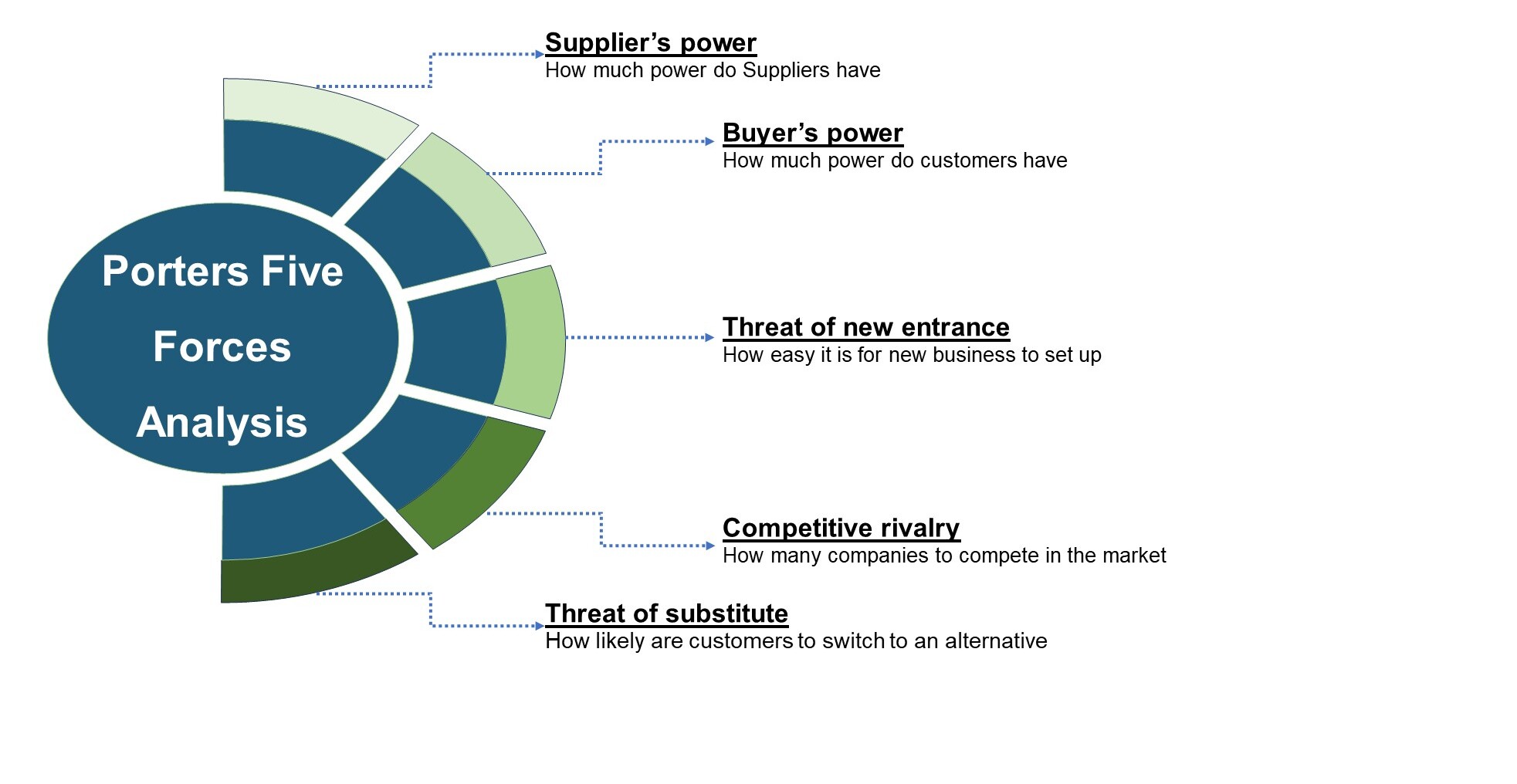
Porters Five Forces Analysis
We conduct Porter's Five Forces analysis to evaluate the competitive landscape of an industry, providing us with insights into factors that affect profitability and strategic positioning.
SWOT Analysis

Forecasting
We utilize a forecasting model to predict future consumption by considering parameters like population, economics, regulations, market competition, drivers, constraints, technology, and pricing. We also employ statistical techniques such as multilinear regression, exponential smoothing, moving average, ARIMA, and Monte Carlo simulations for accurate predictions. In econometric forecasting, we analyzed short-term and long-term event impacts, attributing values based on regulatory frameworks, economic factors, and market events.


 Speak to Our Analyst


 Market")