Market")
Semiconductor Manufacturing Equipment Market By Equipment Type (Patterning & Lithography, Deposition, Etching, Ion Implantation, Thermal Processing, Chemical Mechanical Planarization (CMP), Cleaning & Surface Preparation, Metrology & Inspection, Wafer Bonding & Wafer Level Packaging, Wafer Handling & Automation, Facilities & Fab Infrastructure, Test & Probe (Wafer Sort), and Other Specialty Tools), and Others – Global Opportunity Analysis and Industry Forecast, 2025–2030
Industry Outlook
The global Semiconductor Wafer Fab Equipment (WFE) Market size was valued at USD 94.97 billion in 2024 and is expected to reach USD 101.57 billion by 2025. Looking ahead, the industry is projected to expand significantly, reaching USD 142.11 billion by 2030, registering a CAGR of 7.9% from 2025 to 2030.
The market is expanding rapidly, fuelled by the surging demand for advanced chips in AI, 5G, automotive electronics, and data center applications. Semiconductor manufacturers are heavily investing in cutting-edge wafer fabrication tools to support the transition to smaller process nodes, 3D architectures, and heterogeneous integration. The growing adoption of EUV lithography, atomic layer deposition, and advanced metrology systems is driving equipment innovation and capital spending across foundries and integrated device manufacturers (IDMs). Supply chain diversification, government-backed chip initiatives, and capacity expansions in regions such as the U.S., Taiwan, South Korea, and Europe are further accelerating market momentum. By combining precision engineering, automation, and material science advancements, the semiconductor front-end equipment is enabling next-generation semiconductor production and shaping the future of global technology infrastructure.

The chart shows a sharp increase in the percentage of organisations using AI in at least one function, rising from 20% in 2017 to 78% in 2024, highlighting the mainstream adoption of AI technologies across industries. This sweeping uptake of AI drives exponential demand for high-performance, energy-efficient chips used in AI training and inference, intensifying the need for cutting-edge semiconductor manufacturing technologies. As a result, the semiconductor wafer fab equipment (WFE) market experiences significant growth, propelled by investments in advanced lithography, etching, deposition, and metrology tools required to produce the next generation of logic, memory, and specialised AI accelerators in wafer fabrication plants worldwide.
What Are the Key Trends in the Semiconductor Wafer Fab Equipment (WFE) Industry?
How is WFE Demand Shifting Between Logic, Memory and Advanced Packaging Investments?
SEMI data show that 2024 demand was broad-based, wafer-processing equipment rose, and back-end/assembly & packaging rebounded sharply as advanced packaging and HBM projects accelerated. SEMI specifically highlights that investments in advanced logic, mature logic and advanced packaging drove the recovery, with China, Korea and Taiwan together accounting for roughly three-quarters of equipment spending in 2024. This implies customers are layering capacity expansion for both cutting-edge nodes and for advanced packaging and HBM, creating simultaneous demand across lithography, etch/deposition and packaging toolsets. For equipment vendors, the commercial consequence is portfolio breadth, suppliers with strength across front-end and back-end capture a larger share of multi-project programs. Suppliers are prioritising solutions that reduce total cost-of-ownership across node transitions and secure channel/parts agreements in Asia to translate order leads into installed base semiconductor wafer fab equipment (WFE) market.

The chart presents the Technology Readiness Index by country for 2024, with China (65.3) and Japan (63.8) demonstrating the highest preparedness levels, while India (52.6) and Indonesia (56.1) lag behind. These scores indicate a nation's capability to deploy and leverage advanced technologies, including digital infrastructure, R&D investment, and skilled workforce. Higher technology readiness directly boosts the semiconductor wafer fab equipment (WFE) market demand, as countries better positioned for innovation are more likely to expand semiconductor manufacturing capacity and invest in state-of-the-art wafer fab equipment to support growth in AI, IoT, automotive electronics, and cloud computing sectors.
How are Lithography and EUV Supply Dynamics Shaping Supplier Power and Capex Timing?
EUV lithography remains the bottleneck and strategic choke point at leading nodes, ASML’s 2024 reporting underscores the centrality of EUV systems to leading-edge scaling and the sensitivity of customer ordering to geopolitical and export-control dynamics. ASML’s advanced tool cadence and limited long-lead capacity mean foundries and IDMs must plan multi-year capex cycles, which concentrates supplier leverage and creates order volatility when customers hedge by timing placements. The result is that the semiconductor wafer fab equipment (WFE) market, short-term book-to-bill and quarterly billings show large swings while long-term demand for EUV remains strong. Companies should therefore manage revenue-cycle risk by diversifying service revenue, accelerating refurbished/mid-life tool programmes, and preserving priority capacity for high-margin EUV spares and maintenance contracts. This reduces exposure to order timing and smooths cash flows during cyclical pauses.
How are Geopolitical Export Controls and Regionalisation Altering Supplier Route-To-Market and Risk?
Export-control measures and customer risk-management (notably around China exposure) materially influence equipment ordering patterns and supplier revenue mixes, ASML flagged customer caution in 2024 due to export curbs and expects regional sales shift impacts. SEMI and company filing trends show equipment spending surges in China during 2024, but suppliers must balance compliance risk and long-lead order fulfilment challenges. The practical implication for suppliers and buyers is to strengthen compliance programs, develop regional supply-chain redundancy, and cultivate local service capabilities where permissible. Suppliers are expanding localised service and standardised refurbishment offerings in regions where new-tool shipments are constrained, while pursuing multi-sourcing for critical subcomponents to reduce geopolitical single-point failures.
What Are the Key Market Drivers, Breakthroughs, And Investment Opportunities That Will Shape the Semiconductor Wafer Fab Equipment (WFE) Industry in the Next Decade?
Investment in chip capacity for AI, cloud and high-performance computing is the dominant demand engine, concurrently, memory recoveries and advanced packaging initiatives provide complementary upsides. These drivers combine with supplier concentration and industry policy objectives to create an environment of elevated, but regionally uneven, capital spending. However, export controls, cyclical demand and long lead times create operational complexity for suppliers and customers.
Technological breakthroughs are opening new upgrade paths; buyers face the challenge of precisely timing investments while preserving flexibility across node generations. Capital allocation that blends new-tool purchases with refurbishment and service contracts represents a pragmatic path to reduce unit cost volatility and preserve yield improvement trajectories.
Growth Drivers:
How will Ai-Driven Logic Demand Sustain Semiconductor Wafer Fab Equipment (WFE) Market Growth?
The accelerating AI compute cycle is fuelling sustained demand for leading-edge logic and advanced packaging, driving a new phase of wafer fab equipment (WFE) expansion. According to SEMI 2025 report, worldwide sales of semiconductor manufacturing equipment increased 10% to USD 117.1 billion in 2024. As GPU and accelerator build-outs intensify, capex intensity per fab continues to rise, benefiting suppliers of lithography, etch, deposition, and metrology tools. The shift toward chiplet-based architectures and 3D integration further increases complexity and equipment requirements. To capture long-term semiconductor wafer fab equipment (WFE) market growth, equipment vendors should align product roadmaps with next-generation logic nodes, prioritise yield and overlay precision, and co-develop process innovations with foundries. Strategic partnerships and multi-year procurement agreements will secure predictable revenues amid heightened AI-driven capacity investments.

This chart highlights the 2024 global AI adoption rates by country, with the U.S. at 45%, the UK at 41%, China at 39%, Germany at 36%, and India at 28%. These figures reflect varying degrees of AI penetration into enterprise workflows and suggest an accelerating reliance on advanced computing across major economies. As countries with high AI adoption invest in new technologies and automation, the demand for advanced semiconductor devices and specialised processors (such as AI accelerators) increases, fueling robust growth in the semiconductor wafer fab equipment (WFE) market expansion as manufacturers upgrade and expand wafer fabrication facilities to meet evolving chip performance, complexity, and volume requirements.
How will Memory (DRAM/NAND/HBM) Cycles Contribute to WFE Spending?
The recovery in memory capital expenditures is a critical tailwind for semiconductor WFE market, supported by renewed investment in DRAM, NAND, and high-bandwidth memory (HBM) technologies. As AI workloads demand greater bandwidth and energy efficiency, memory makers are accelerating transitions to advanced stacking and 3D architectures, driving the need for high-throughput deposition, etch, and packaging tools. Equipment suppliers offering productivity gains and yield optimisation for memory processes are positioned to capture disproportionate share during cyclical upturns. To maximise impact, vendors should focus on scalable production tools, strengthen engagements with customers by building multi-fab memory clusters, and align capacity plans with the next memory expansion cycle.
Growth Inhibitors:
How do Long Lead Times and Supply-Chain Constraints Limit Market Responsiveness?
Long lead times for complex tools, concentrated sub-component suppliers and logistical constraints create order backlog volatility and defer customer rollouts. ASML and other vendors reported order timing sensitivity and client caution, underscoring how supply rhythm mismatch and export compliance delay revenue recognition. To mitigate, firms should expand refurbishment and spare-parts programs, flex manufacturing capacity between high-margin and aftermarket offerings, and strengthen supplier diversification for critical optics, lasers and vacuum components. This reduces single-point risks and smooths revenue through cycles.
Where Should Investors Allocate to Capture Durable Returns?
High-conviction investment areas include specialised process control and metrology, aftermarket service and spare parts, and companies enabling advanced packaging and HBM. SEMI’s market rebound in 2024 and supplier filings emphasise the value of firms that convert technological leadership into serviceable installed bases. Investors should prioritise suppliers with strong IP portfolios and diversified geographical service networks, and those with validated co-development agreements with leading foundries and memory producers to de-risk demand cyclicality.
How Semiconductor Wafer Fab Equipment Market Segmented in This Report, And What Are the Key Insights from the Segmentation Analysis?
By Equipment Type Insights
Is Lithography Dominating Equipment Type Demand in 2025?
Based on equipment type, the market is segmented into lithography equipment, deposition equipment, etching equipment, cleaning equipment, and others.
Lithography, particularly EUV for leading nodes and DUV for mature nodes, remains the single most strategic equipment category because it sets scaling capability and largely determines fab node roadmaps. ASML’s emphasis on EUV and computational lithography in its 2024 annual report reflects this centrality. As a result, lithography vendors hold structural pricing power, fabs’ timing for node transitions directly drives lithography order cycles. Fabs and vendors are aligning on multi-year capacity commitments and spare parts/service agreements to manage the long procurement and installation horizons associated with lithography systems.
By Process Node Insights
Is the Advanced Node Segment the Primary Process-Node Growth Driver?
Based on the process node, the market is segmented into advanced node, mid node, and mature node.
Advanced nodes command outsized capital intensity as demand from AI/accelerator workloads increases. Company filings and SEMI market statistics show front-end tools for leading-edge logic and related metrology experienced the strongest investment growth in 2024. This elevates suppliers with leading-edge tool portfolios, but it also raises customers’ sensitivity to supply constraints and export controls. Vendors are locking strategic multi-fab partnerships and prioritising high-value feature deliveries (throughput, overlay) that accelerate customer node ramps.
By Wafer Size Insights
Is 300 mm Wafer Equipment Dominating Capex Allocation?
Based on wafer size, the market is segmented into 150 mm, 200 mm, 300 mm, and above 300 mm.
300mm fabs continue to dominate capital allocation for mainstream high-volume logic and memory expansion because wafer-area economics favour larger diameters for advanced nodes. SEMI’s 2024 equipment analysis and major supplier financials reflect that the largest order flows and highest-value tooling are 300 mm-centric. Vendors should therefore prioritise 300mm tool throughput and uptime innovations while maintaining focused offerings for 200mm niches (power, MEMS) that provide steady aftermarket revenue. A dual-tier product strategy protects installed-base profitability and serves cross-segment demand.
By Application Insights
Is Logic and Foundry the Largest Application Segment in 2025?
Based on application, the market is segmented into logic and foundry, memory (including DRAM and NAND flash), power devices, analog and mixed signal devices, sensors and MEMS, and others.
Logic and foundry applications drove a significant portion of semiconductor wafer fab equipment (WFE) market in 2024, supported by expansion among foundries building capacity for AI-centric chips. SEMI notes leading-edge logic and advanced packaging as key demand pillars. This favours full-stack suppliers that provide lithography, deposition, etch and inspection solutions to foundries. Equipment vendors are structuring dedicated foundry engagement teams to support multi-site, multi-node rollouts and bundle service contracts that guarantee yield ramp support.
By End User Insights
Is the IDM / Foundry End-User Split Favouring Foundries for New Capex?
Based on end user, the market is segmented into integrated device manufacturers (IDMs), foundries, memory manufacturers, outsourced semiconductor assembly and test (OSAT) companies, research and development laboratories, and speciality device manufacturers.
Foundries and large memory manufacturers were the primary new-capex drivers in 2024, supported by national and corporate programs to expand capacity, IDMs remain significant buyers but balance capex across in-house and outsourced options. SEMI regional breakdowns show Asia's foundry and memory projects concentrate most spend. Suppliers should tailor commercial models to foundry multi-fab needs (volume discounts, guaranteed throughput) while retaining IDM-focused premium services for long-term support agreements.
Regional Outlook
The semiconductor wafer fab equipment (WFE) market share is geographically studied across North America, Europe, Asia Pacific, Middle East & Africa, and Latin America and each region is further studied across countries.
Semiconductor Wafer Fab Equipment (WFE) Market in North America
North America remains a pivotal hub for semiconductor wafer fab equipment (WFE) market, supported by advanced logic, speciality fabs, and process control expansion. The region benefits from strong government incentives, particularly through the U.S. CHIPS and Science Act, which is accelerating foundry and equipment ecosystem growth. Major suppliers with established U.S. service networks gain an advantage through proximity to leading-edge fabs and integrated partnerships with system-on-chip and packaging innovators. Equipment demand focuses on metrology, inspection, and automation tools that enhance yield and process reliability. Continued investment in domestic manufacturing resilience positions North America as a strategic anchor in the global semiconductor supply chain.
Semiconductor Wafer Fab Equipment (WFE) Market in the United States
The United States leads North American market trends, driven by large-scale investments in foundries, logic nodes, and advanced packaging facilities under CHIPS Act funding. Equipment spending emphasises lithography, metrology, and process control systems needed for 5 nm and below nodes. U.S.-based service and compliance capabilities provide differentiation, ensuring operational uptime and adherence to export control standards. Collaborations between equipment vendors, national labs, and emerging foundry operators are expanding technology access while securing domestic semiconductor sovereignty. The U.S. continues to position itself as both a leading end market and a manufacturing hub for next-generation wafer fabrication technologies.
Semiconductor Wafer Fab Equipment (WFE) Market in Canada
Canada’s market remains modest in scale but strategically relevant for niche semiconductor applications, speciality materials, and academic research. The country’s strengths lie in R&D collaborations between universities, startups, and government laboratories focused on photonics, sensors, and compound semiconductors. Equipment demand centers on pilot and speciality tools that support research-grade and low-volume manufacturing. With supportive public funding and increasing participation in North American semiconductor supply chain initiatives, Canada presents growth opportunities for specialised toolmakers seeking to partner in innovation-driven segments.
Semiconductor Wafer Fab Equipment (WFE) Market in Europe
Europe’s market is expanding under its semiconductor sovereignty and strategic autonomy agenda. The EU Chips Act is spurring investment in both logic and advanced packaging capabilities, creating new opportunities for equipment suppliers across lithography, automation, and materials handling. The region’s complex regulatory and operational environment favours vendors with robust service and installation support. Germany, France, and the Netherlands anchor the continent’s semiconductor production, while cross-border collaborations enhance regional supply chain resilience. As Europe focuses on high-value manufacturing, demand for precision tools and sustainable fab operations continues to accelerate.
Semiconductor Wafer Fab Equipment (WFE) Market in the United Kingdom
The U.K. represents a smaller but technologically advanced segment of the global semiconductor wafer fab equipment (WFE) market , emphasising semiconductor research, design, and speciality manufacturing. Investments focus on pilot-scale fabs and R&D centers dedicated to compound semiconductors, photonics, and power devices. Equipment needs to concentrate on advanced metrology and process tools suited to low-volume innovation environments. Strategic collaborations between academia, startups, and global equipment vendors are fostering technology transfer and skill development, positioning the U.K. as an innovation node within the broader European semiconductor ecosystem.
Semiconductor Wafer Fab Equipment (WFE) Market in Germany
Germany remains the industrial backbone of Europe’s semiconductor equipment demand, driven by its precision manufacturing ecosystem and role in EU industrial policy. Strong activity in specialty fabs, power semiconductors, and automotive electronics sustains steady demand for metrology, deposition, and automation tools. Government-backed initiatives under the European Chips Act continue to enhance R&D and manufacturing capabilities. Equipment vendors that offer localised technical service and comply with Germany’s stringent industrial standards benefit from long-term engagement with major regional fabs and OEM partners.
Semiconductor Wafer Fab Equipment (WFE) Market in France
France is emerging as a central player in Europe’s semiconductor reindustrialisation strategy, emphasising R&D, advanced packaging, and automation. National initiatives under the France 2030 plan and the EU Chips Act are channelling investments into local fab expansions and pilot lines. Equipment demand focuses on lithography, process control, and packaging tools that support mixed-signal and speciality semiconductor production. Partnerships between CEA-Leti, STMicroelectronics, and global tool vendors are driving innovation in 3D integration and wafer-level packaging. France’s blend of research strength, industrial policy support, and technology partnerships positions it as a critical node in Europe’s advanced semiconductor ecosystem.
Semiconductor Wafer Fab Equipment (WFE) Market in Italy
Italy’s semiconductor sector is gaining strategic importance through investments in speciality and power semiconductors aligned with automotive and industrial applications. Supported by EU and national funding, Italy is strengthening its role in design, assembly, and packaging activities rather than large-scale logic manufacturing. Equipment demand is oriented toward deposition, etch, and metrology tools that enhance power device fabrication and materials research. Collaboration between universities, public research institutions, and European equipment suppliers continues to expand local innovation capacity. As Italy integrates further into EU semiconductor value chains, opportunities will grow for specialised tool providers and service partners targeting sustainable and energy-efficient production.
Semiconductor Wafer Fab Equipment (WFE) Market in Spain
Spain’s semiconductor ambitions are evolving under the PERTE Chip program, an initiative aimed at strengthening domestic design, R&D, and limited fabrication capacity. The market currently emphasises research-grade and pilot-scale wafer equipment to support photonics, MEMS, and compound semiconductor projects. Strategic collaborations between universities, technology institutes, and global equipment manufacturers are enhancing local capabilities in process automation and material deposition. While Spain remains an emerging player, its policy-driven investments and industrial partnerships are laying the foundation for long-term ecosystem development. Equipment vendors that engage early with these public-private initiatives will be best positioned for future growth opportunities.
Semiconductor Wafer Fab Equipment (WFE) Market in the Nordics
The Nordic region, comprising Sweden, Finland, Denmark, and Norway, plays a crucial role in Europe’s semiconductor innovation network through its focus on advanced materials, photonics, and automation. Supported by strong government R&D funding and industrial collaboration, Nordic countries host several research fabs and packaging pilot projects. Equipment demand centers on process metrology, thin-film deposition, and advanced lithography for prototype-scale production. Companies such as VTT, RISE, and Lund Nano Lab drive partnerships between academia and global toolmakers. The region’s emphasis on sustainability, precision manufacturing, and digital automation positions it as a leader in next-generation semiconductor research and pilot-scale fabrication within Europe.
Semiconductor Wafer Fab Equipment (WFE) Market in the Asia-Pacific
Asia-Pacific dominates global semiconductor wafer fab equipment (WFE) market investment, accounting for the majority of worldwide equipment spending. China, South Korea, and Taiwan lead in foundry and memory expansion, while Japan maintains strength in precision tool manufacturing and materials technology. The region’s rapid capacity build-up is driven by both government subsidies and private investments targeting advanced nodes and packaging. Equipment suppliers face a dual imperative, capturing demand from high-growth markets while maintaining trade-policy compliance and technology transfer controls. APAC’s scale and ecosystem maturity ensure it remains the epicentre of global semiconductor manufacturing.
Semiconductor Wafer Fab Equipment (WFE) Market in China
China remains the largest single-country semiconductor wafer fab equipment (WFE) market, propelled by aggressive government incentives to expand domestic semiconductor capacity. National and provincial funding programs continue to support logic, memory, and power-device fabs, driving robust demand for deposition, etch, and inspection tools. However, export restrictions and compliance considerations shape vendor participation. Success depends on localised partnerships, after-sales service networks, and technology alignment with regulatory boundaries. Despite geopolitical constraints, China’s long-term commitment to semiconductor self-sufficiency ensures sustained equipment demand across multiple technology tiers.
Semiconductor Wafer Fab Equipment (WFE) Market in Japan
Japan remains a cornerstone of the global semiconductor ecosystem, excelling in both equipment manufacturing and advanced materials. The nation’s focus on precision engineering and R&D leadership sustains strong domestic demand for deposition, metrology, and inspection tools. Government-backed programs under the Economic Security Promotion Act are reinforcing local production of leading-edge logic and memory, with major investments from global players such as TSMC and Rapidus. Japan also plays a key role in developing advanced packaging and 3D integration technologies. Equipment vendors benefit from close collaboration with Japanese fabs and suppliers, ensuring continuous innovation and maintaining Japan’s status as a technology leader in the semiconductor value chain.
Semiconductor Wafer Fab Equipment (WFE) Market in India
India’s semiconductor equipment market is in an early but fast-evolving stage, driven by strong government support through the India Semiconductor Mission and production-linked incentive (PLI) schemes. The country’s ambitions to establish local fabrication and assembly facilities are creating an emerging demand for lithography, etch, and metrology tools. While large-scale fab operations are still developing, growing investment from global foundries and domestic conglomerates is expanding pilot and research-scale activities. Equipment vendors entering India benefit from policy incentives, infrastructure partnerships, and workforce development programs. As the ecosystem matures, India is poised to become a strategic hub for advanced packaging, testing, and design-centric manufacturing within South Asia.
Semiconductor Wafer Fab Equipment (WFE) Market in South Korea
South Korea remains a global powerhouse in semiconductor manufacturing, anchored by major memory and logic producers investing heavily in next-generation capacity. High-bandwidth memory (HBM), 3D NAND, and logic process transitions are driving strong demand for deposition, etch, and cleaning equipment. Government initiatives supporting domestic equipment localisation and R&D collaboration with industry leaders further reinforce supply chain resilience. Vendors with advanced process control, high-throughput, and yield-enhancement capabilities are well-positioned to capture market share. South Korea’s continued focus on AI-driven chip architectures, coupled with significant fab expansions by leading companies, ensures sustained wafer fab equipment growth across memory and logic segments.
Semiconductor Wafer Fab Equipment (WFE) Market in Indonesia
Indonesia’s semiconductor ecosystem is at a formative stage, emphasising foundational investments in electronics manufacturing and materials processing. The government’s Making Indonesia 4.0 roadmap promotes digital industrialisation and local capacity building for electronics, sensors, and assembly operations. Current WFE demand remains limited to test, measurement, and small-scale R&D tools, but growing public-private partnerships indicate long-term potential for packaging and component production. Collaboration with global technology firms and support from development agencies are helping strengthen local infrastructure. For equipment suppliers, Indonesia offers early-stage engagement opportunities through technical training, pilot installations, and participation in national semiconductor capability-building programs.
Semiconductor Wafer Fab Equipment (WFE) Market in Australia
Australia’s semiconductor wafer fab equipment (WFE) industry is modest but strategically oriented toward advanced research, materials science, and defence-related semiconductor applications. National investments through initiatives like the AUKUS technology collaboration and CSIRO’s advanced manufacturing programs are fostering specialised semiconductor R&D ecosystems. Universities and innovation hubs across Sydney, Melbourne, and Canberra are driving pilot-scale fabrication in quantum computing, photonics, and compound semiconductors. Equipment demand centers on precision deposition, lithography, and metrology tools tailored for prototype and research use. Australia’s strong research base and emphasis on trusted supply chains position it as a niche but valuable partner within the global semiconductor innovation network.
Semiconductor Wafer Fab Equipment (WFE) Market in Latin America
Latin America remains an emerging but strategically evolving region in the global semiconductor landscape, with increasing interest in localising electronics manufacturing and fostering R&D collaboration. Countries such as Brazil and Mexico are advancing semiconductor initiatives through technology parks, government incentives, and partnerships with international chipmakers. Current WFE demand primarily centers on assembly, testing, and pilot-scale fabrication tools. Growing investments in electric vehicles, renewable energy, and industrial automation are creating downstream opportunities for sensor and power semiconductor development. Equipment suppliers entering this region benefit from academic partnerships, technology transfer programs, and early participation in regional semiconductor ecosystem development.
Semiconductor Wafer Fab Equipment (WFE) Market in the Middle East & Africa
The Middle East and Africa (MEA) are at an early stage of semiconductor ecosystem development but show rising interest in high-tech manufacturing and localization of critical technologies. The Gulf states, particularly the UAE and Saudi Arabia, are investing in digital transformation visions to build advanced electronics and chip-design capabilities. WFE demand in the region is largely focused on testing, metrology, and research-scale equipment supporting pilot and academic facilities. In Africa, South Africa and Egypt lead efforts in electronics assembly and materials research. For global suppliers, MEA represents a frontier market with potential for R&D partnerships, skill-building collaborations, and technology diversification aligned with national innovation agendas.
Competitive Landscape
Which Companies Dominate the Semiconductor Wafer Fab Equipment (WFE) Industry and How do they Compete?
Leading companies in the semiconductor wafer fab equipment (WFE) industry, such as ASML Holding N.V., Applied Materials, Inc., Lam Research Corporation, Tokyo Electron Ltd., KLA Corporation, ASM International N.V., SCREEN Holdings Co., Ltd., Nikon Corporation, Canon Inc., Veeco Instruments Inc., AIXTRON SE, Axcelis Technologies, Inc., EV Group Europe & Asia/Pacific GmbH, SUSS MicroTec SE, Onto Innovation, Inc., Daifuku Co., Ltd., EBARA Corporation, FormFactor, Inc., Advantest Corporation, and Teradyne, Inc. have established themselves as key players through strategic acquisitions and global expansion.
Market Dominated by Semiconductor Wafer Fab Equipment (WFE) Giants and Specialists
Competition is structured around a small set of large, technology-intensive firms and a broader set of specialized vendors. ASML retains strategic dominance in lithography (especially EUV), giving it outsized influence on leading-edge node timelines. Applied Materials and Lam Research compete across deposition, etch and process integration, KLA dominates process-control and metrology. Tokyo Electron and SCREEN provide broad portfolios that capture diverse regional demand. The competitive balance rests on technology leadership, IP protection, and the ability to supply integrated tool chains that reduce fab ramp risk for customers.
Innovation and Adaptability Drive Market Success
Companies that convert R&D into measurable throughput/yield gains win multi-fab contracts, filings show suppliers expanding computational control, advanced metrology, and service ecosystems to lock in customers. For example, suppliers report expanding service and refurbished tool programmes to stabilise revenue amid order cycles. Vendors should accelerate software and digital services to turn installed bases into recurring high-margin revenue streams. Partnerships with foundries on co-development of node-specific process recipes further strengthen competitive moats.
Market Players to Opt for Merger & Acquisition Strategies to Expand their Presence
M&A and strategic partnerships remain active playbooks to acquire niche capabilities, inspection, packaging automation, and to extend geographic service networks. Supplier filings and investor communications show continued focus on tuck-ins and technology acquisitions that fill product-portfolio gaps or accelerate entry into aftermarket services. Investors should track consolidation that reduces component-level single-supplier risks and that bundles inspection plus process tools, these combined offerings gain preference from fabs seeking simplified integration and single-vendor accountability.
List of Key Semiconductor Wafer Fab Equipment (WFE) Companies
-
ASML Holding N.V.
-
Applied Materials, Inc.
-
Lam Research Corporation
-
Tokyo Electron Ltd.
-
KLA Corporation
-
ASM International N.V.
-
SCREEN Holdings Co., Ltd.
-
Nikon Corporation
-
Canon Inc.
-
Veeco Instruments Inc.
-
AIXTRON SE
-
Axcelis Technologies, Inc.
-
EV Group Europe & Asia/Pacific GmbH
-
SUSS MicroTec SE
-
Onto Innovation, Inc.
-
Daifuku Co., Ltd.
-
EBARA Corporation
-
FormFactor, Inc.
-
Advantest Corporation
-
Teradyne, Inc.
What Are the Latest Key Industry Developments?
-
September 2025 - ASML Holding N.V. expanded its High-NA EUV lithography technology roadmap by introducing advanced semiconductor manufacturing solutions designed for sub-2nm process nodes. The company focused on improving transistor density, production precision, and chip performance for AI, high-performance computing (HPC), and advanced mobile semiconductor applications. This development is expected to strengthen next-generation semiconductor fabrication capabilities globally.
-
August 2025 - Applied Materials, Inc. launched new AI-enabled semiconductor fabrication and advanced packaging solutions aimed at improving wafer yield, process efficiency, and chip performance. The company emphasized technologies supporting heterogeneous integration, advanced memory architectures, and energy-efficient semiconductor manufacturing processes for AI and data center applications.
-
July 2025 - Lam Research Corporation introduced advanced dry resist processing and atomic layer etching technologies to support next-generation semiconductor nodes and 3D device architectures. The company focused on enabling higher precision manufacturing and improved process control for leading-edge logic and memory semiconductor production.
What Are the Key Factors Influencing Investment Analysis & Opportunities in the Semiconductor Wafer Fab Equipment (WFE) Market?
Investment analysis should prioritise revenue durability (installed-base services and spare parts), technology leadership (patented optics, EUV components, metrology IP), and geopolitical exposure (customer concentration in China vs. compliant markets). SEMI’s 2024 market rebound highlights the cyclicality and regional concentration of spend, therefore, valuation must incorporate scenario analyses for order timing and export-control scenarios. High-return hotspots include process control/metrology firms (yield improvement leverage), aftermarket services/refurbishment, and equipment enabling advanced packaging and HBM. Investors should stress-test business models on backlog sensitivity, percentage of recurring revenue, and strength of long-term OEM customer agreements.
Key Benefits for Stakeholders:
Next Move Strategy Consulting (NMSC) presents a comprehensive analysis of the semiconductor wafer fab equipment (WFE) market trends, covering historical trends from 2020 through 2024 and offering detailed forecasts through 2030. Our study examines the market at regional and country levels, providing quantitative projections and insights into key growth drivers, challenges, and investment opportunities across all major wafer fabrication equipment segments.
Investors gain exposure to secular chip demand (AI, cloud, mobility) with diversified return paths via new-tool cycles and recurring service streams, customers (foundries, IDMs, memory fabs) benefit from higher throughput and yield as suppliers innovate in metrology and process tools. Aligning commercial models to produce measurable yield and uptime improvements translates to faster ROI for fab owners and recurring margin capture for equipment vendors.
Report Scope
|
Parameters |
Details |
|
Market Size in 2025 |
USD 101.57 Billion |
|
Revenue Forecast in 2030 |
USD 142.11 Billion |
|
Growth Rate |
CAGR of 7.9% from 2025 to 2030 |
|
Analysis Period |
2024–2030 |
|
Base Year Considered |
2024 |
|
Forecast Period |
2025–2030 |
|
Market Size Estimation |
Billion (USD) |
|
Growth Factors |
|
|
Companies Profiled |
15 |
|
Countries Covered |
33 |
|
Market Share |
Available for 10 companies |
|
Customization Scope |
Free customization (equivalent to up to 80 analyst-working hours) after purchase. Addition or alteration to country, regional & segment scope. |
|
Pricing and Purchase Options |
Avail customized purchase options to meet your exact research needs. |
|
Approach |
In-depth primary and secondary research; proprietary databases; rigorous quality control and validation measures. |
|
Analytical Tools |
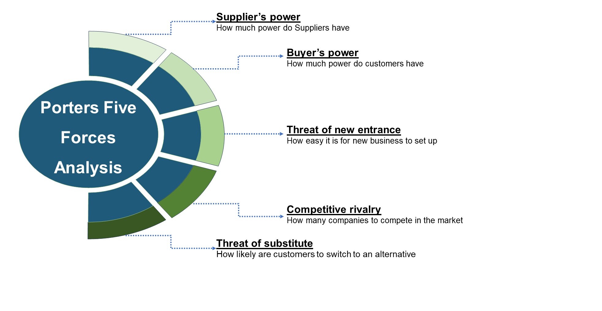
Porter's Five Forces, SWOT, value chain, and Harvey ball analysis to assess competitive intensity, stakeholder roles, and relative impact of key factors. |
Key Market Segments
By Equipment Type
-
Patterning & Lithography
-
EUV Lithography Systems
-
DUV Lithography Systems
-
ArF Immersion
-
ArF Dry
-
KrF & Legacy DUV
-
-
Coater & Developer (Track)
-
Mask & Reticle Manufacturing Equipment
-
-
Deposition
-
Chemical Vapor Deposition (CVD)
-
PECVD
-
LPCVD
-
-
Physical Vapor Deposition (PVD)
-
Atomic Layer Deposition (ALD)
-
Epitaxy (Epi Reactors)
-
Electroplating & Metal Fill
-
-
Etching
-
Dry Etch
-
Wet Etch
-
-
Ion Implantation
-
High Current Implanters
-
Medium Current Implanters
-
High Energy Implanters
-
-
Thermal Processing
-
Rapid Thermal Processing (RTP)
-
Diffusion & Oxidation Furnaces
-
Laser Anneal
-
-
Chemical Mechanical Planarization (CMP)
-
Cleaning & Surface Preparation
-
Single Wafer Cleaning Systems
-
Batch Cleaning Systems
-
-
Metrology & Inspection
-
Critical Dimension Metrology
-
Overlay Metrology
-
Thin Film & Film Thickness Metrology
-
Defect Inspection & Review
-
Materials & Composition Metrology
-
-
Wafer Bonding & Wafer Level Packaging
-
Bonding & Align Systems
-
TSV Processing & Redistribution Layer
-
WLP-specific Deposition & Inspection
-
-
Wafer Handling & Automation
-
Front End Automation & (AMHS)
-
Robotics & FOUP Loaders
-
Vacuum & Gas Delivery Subsystems
-
-
Facilities & Fab Infrastructure
-
Gas & Chemical Delivery Systems
-
Cleanroom Modules & Environmental Controls
-
-
Test & Probe (Wafer Sort)
-
Other Specialty Tools
By Process Technology Node
-
Leading Edge (<7 nm)
-
Advanced (7 nm - 14 nm)
-
Mainstream (16 nm - 28 nm)
-
Mature (>28 nm)
-
Specialty Processes
-
Power & SiC/GaN
-
MEMS & Sensors
-
Photonics & Optoelectronics
-
By Wafer Size
-
300 mm
-
200 mm
-
≤150 mm
-
450 mm (Pilot & Development)
By Primary Semiconductor Application
-
Foundry & Logic
-
Leading-Edge Logic (AI, HPC, Mobile)
-
Mature & Specialty Logic (Auto, IoT)
-
-
Memory
-
Dynamic Random-Access Memory (DRAM)
-
High-Bandwidth Memory (HBM)
-
Mainstream DRAM
-
-
NAND Flash Memory
-
-
Power & Analog
-
Power Discretes (SiC, GaN)
-
Analog & Mixed-Signal
-
-
Sensors & MEMS
-
Photonics & Optoelectronics
-
Other Specialty Devices
By Revenue Type
-
New Equipment Sales
-
Aftermarket & Recurring Revenue
-
Maintenance Contracts & Services
-
Spare Parts & Repairs
-
Consumables & Process Materials
-
Refurbished & Used Equipment
-
-
Software & Digital Services
-
Process Control & Yield Management Software
-
Remote Monitoring & Predictive Analytics
-
Performance & Optimization Services
-
By Buyer Type
-
Pure-Play Foundries
-
Integrated Device Manufacturers (IDMs)
-
Memory Manufacturers
-
Outsourced Assembly & Test (OSAT) Providers
-
Research & Pilot Fabs
Geographical Breakdown
-
North America: U.S., Canada, and Mexico.
-
Europe: U.K., Germany, France, Italy, Spain, Sweden, Denmark, Finland, Netherlands, and rest of Europe.
-
Asia Pacific: China, India, Japan, South Korea, Taiwan, Indonesia, Vietnam, Australia, Philippines, Malaysia and rest of APAC.
-
Middle East & Africa (MEA): Saudi Arabia, UAE, Egypt, Israel, Turkey, Nigeria, South Africa, and rest of MEA.
-
Latin America: Brazil, Argentina, Chile, Colombia, and rest of LATAM
Conclusion & Recommendations
Our report equips stakeholders, industry participants, investors, and consultants with actionable intelligence to capitalise on Semiconductor Wafer Fab Equipment (WFE)’s transformative potential. By combining robust data-driven analysis with strategic frameworks, NMSC’s Semiconductor Wafer Fab Equipment (WFE) Market Report serves as an indispensable resource for navigating the evolving landscape.
The semiconductor wafer fab equipment (WFE) market re-entered a constructive growth phase led by AI-driven logic demand and memory recoveries, with Asia (China, Korea, Taiwan) the dominant regional spender. Supplier advantage accrues to firms that combine technological leadership (EUV, metrology), robust regional service networks, and flexible product strategies across 200mm/300mm footprints. Export controls inject risk that suppliers must manage through compliance, local service expansion and refurbished/refit programs.
 Market Revenue by 2030 (Billion USD)")
 Market Segmentation")
About the Author
 Ridip Gogoi is a research associate recognized for his strong analytical thinking and meticulous attention to detail. He specializes in transforming complex datasets into meaningful insights that support informed business decisions and strategic planning. With a proactive mindset and strong commitment to accuracy, he contributes effectively to market analysis, data validation, and insight generation. Ridip is driven by continuous learning and consistently works to enhance research quality, analytical depth, and reporting clarity across projects.
About the Reviewer
 Supradip Baul is an accomplished business consultant and strategist with over a decade of rich experience in market intelligence, strategy, technology, and business transformation. His work has included rigorous qualitative and quantitative analysis across multiple industries, helping clients shape investment decisions and long-term roadmaps. Earlier in his career, he was associated with Gartner, where he contributed to industry-leading reports and market share analyses. He has worked with leading global companies and holds an MBA with a dual specialization in Marketing and Finance.
At Next Move Strategy Consulting, we understand that insightful market research is the cornerstone of successful business decisions. That's why we employ a robust and multifaceted approach, combining various methodologies to deliver the most accurate and actionable data for our clients.

Research Landscape
We navigate the world of research with two primary approaches:
Qualitative Approach
Our qualitative research methodologies involve immersive techniques such as in-depth interviews, focus groups, and observational studies. By engaging directly with individuals and stakeholders, we uncover valuable insights that quantitative data alone may overlook.

Quantitative Research
In tandem with qualitative methodologies, NMSC leverages the power of Quantitative Research to provide a robust foundation of numerical insights. Through systematic data collection and analysis, we quantify patterns, preferences, and market trends, offering a comprehensive view of the business landscape.
Our quantitative research approach employs diverse tools, including surveys, experiments, and statistical modelling. These methodologies enable us to gather data from a large and representative sample, ensuring the statistical significance of our findings. By employing structured questionnaires and standardized data collection methods, we guarantee the reliability and validity of the information we present to our clients.
Quantitative research is particularly effective in measuring the prevalence of trends, assessing market size, and gauging the impact of various factors on consumer behavior. The numerical precision attained through this approach equips our clients with actionable insights, facilitating data-driven decision-making and strategy formulation.


Our Specialized Toolbox for Industry-Specific Market Research
We deploy a specialized arsenal of techniques tailored to meet your unique requirements. Here's a glimpse into our comprehensive toolbox:

Information Procurement
The stage entails acquiring market data or relevant information through various sources and methodologies.


Market Research Approach
We utilize both top-down and bottom-up approaches in market research analysis to achieve a comprehensive understanding of the market dynamics, leveraging the broad perspective of industry trends and macroeconomic factors alongside detailed insights from specific segments and individual companies.

Porters Five Forces Analysis
We conduct Porter's Five Forces analysis to evaluate the competitive landscape of an industry, providing us with insights into factors that affect profitability and strategic positioning.
SWOT Analysis

Forecasting
We utilize a forecasting model to predict future consumption by considering parameters like population, economics, regulations, market competition, drivers, constraints, technology, and pricing. We also employ statistical techniques such as multilinear regression, exponential smoothing, moving average, ARIMA, and Monte Carlo simulations for accurate predictions. In econometric forecasting, we analyzed short-term and long-term event impacts, attributing values based on regulatory frameworks, economic factors, and market events.


 Speak to Our Analyst