Backside PDN Market Size, Share, Growth & Forecast By Component (Equipment, Materials and Consumables, Software and IP, Services), By Architecture (Buried Power Rail, Backside Via, Direct Backside Contact, Full Backside PDN), By Technology Node (3nm and Below, 4-5nm, Above 5nm, Research and Pilot), By End Use (HPC and AI, Mobile, Client Computing, Automotive, Industrial and IoT), By Customer Type (Foundry, IDM, Fabless, OSAT, Research Institute), and By Sales Channel — Global Analysis 2026–2035
Industry: Semiconductor & Electronics | Publishing Date: July 6, 2026 | Last Updated: September 30, 2026 | No of Pages: N/A | No. of Tables: N/A | No. of Figures: N/A | Format: PDF | Report Code: SE4971
What Is the Backside PDN Market Size?
The global Backside PDN Market was valued at USD 1.2 billion in 2025 and is expected to reach USD 1.5 billion in 2026. Sustained scaling of advanced semiconductor nodes, rising complexity of power delivery networks in leading-edge chips, and accelerating HPC and AI compute deployments are projected to propel the Market to USD 8.6 billion by 2035, advancing at a CAGR of 21.8% from 2026 to 2035. Key growth drivers include the broad adoption of buried power rail architectures at 2nm and below, surging demand for high-performance computing platforms in data centers, expanding AI accelerator production by foundries, and intensifying investment in EDA and physical verification tooling for backside power integrity signoff.
|
Parameters |
Details |
|
Market Size in 2025 |
USD 1.2 Billion |
|
Market Size in 2026 |
USD 1.5 Billion |
|
Revenue Forecast in 2035 |
USD 8.6 Billion |
|
Growth Rate |
CAGR of 21.8% from 2026 to 2035 |
|
Analysis Period |
2025–2035 |
|
Base Year Considered |
2025 |
|
Forecast Period |
2026–2035 |
|
Market Size Estimation |
USD Billion |
|
Companies Profiled |
20 |
|
Countries Covered |
33 |
|
Market Share |
Top 10 |
Backside PDN Market Overview
What Is the Backside PDN Market?
The Backside PDN Market encompasses the ecosystem of semiconductor equipment, materials and consumables, software and IP tools, and specialized services required to design, fabricate, and validate power delivery networks routed through the backside of silicon wafers. Unlike conventional frontside interconnect stacks, backside power delivery decouples signal routing from power distribution, dramatically reducing IR drop, enabling smaller standard cell footprints, and improving power efficiency in leading-edge logic nodes below 5 nanometers. NMSC's analysis indicates that this structural innovation is rapidly becoming a prerequisite for competitive performance in advanced AI accelerators, mobile SoCs, and high-performance computing processors.
How Has the Backside PDN Market Evolved?
From our research, we found that the Backside PDN Market has transitioned through distinct development phases driven by the fundamental limits of conventional frontside power delivery. Early academic and consortium-level research explored buried power rail concepts as a theoretical solution to power density challenges at sub-5nm nodes. The second phase saw process development programs at IMEC and leading foundries validate buried power rail integration at 2nm-class technology nodes. NMSC's analysis indicates that the current phase is characterized by commercial tool qualification, equipment procurement at volume production fabs, and EDA vendor development of dedicated power integrity signoff flows for backside architectures, marking the transition from research prototype to production readiness.
How Do Regulations Influence the Backside PDN Market?
Through our market assessment, we observed that regulatory and policy frameworks are increasingly shaping investment patterns and supply chain dynamics within the Backside PDN Market. National semiconductor industrial policies, including the U.S. CHIPS and Science Act, the European Chips Act, and Japan's semiconductor revival programs, are directing capital toward advanced node fabrication facilities where backside power delivery is a critical process module. Export control regulations under the U.S. Export Administration Regulations restrict the transfer of advanced semiconductor manufacturing equipment and technology to certain jurisdictions, influencing equipment supplier market access and customer qualification timelines for backside PDN process steps.
How Is Technology Adoption Expanding Across the Backside PDN Market?
Technology adoption across the Backside PDN Market is accelerating as leading foundries and integrated device manufacturers formalize their roadmaps for backside power delivery at 2nm and below. Based on our market evaluation, we noticed that TSMC's N2P and A16 process nodes, Intel's 14A node featuring PowerVia technology, and Samsung's SF2 generation all incorporate backside power delivery as a differentiated capability. Equipment suppliers are qualifying dedicated grinding, polishing, lithography, etch, and metallization tools for backside processing flows. Simultaneously, EDA vendors including Synopsys and Cadence are releasing dedicated power integrity and physical verification platforms to support design-technology co-optimization for backside PDN architectures.
|
Key Takeaways |
|
By Component, the Equipment segment held the largest share of the Backside PDN Market at USD 0.62 billion in 2025. Wafer Preparation Equipment and Backside Metallization Equipment collectively account for over 55% of equipment revenue, driven by volume ramp at advanced node fabs requiring dedicated grinding, thinning, barrier deposition, and electroplating tools. |
|
Among Equipment sub-segments, the Metrology and Inspection Equipment sub-category is the fastest-growing at a CAGR of 23.4% from 2026 to 2035, as overlay, defect inspection, and thickness metrology become critical yield gates for backside process integration at 2nm and below nodes. |
|
By Component, Materials and Consumables is the second-largest segment at USD 0.38 billion in 2025, dominated by CMP slurries, dielectric materials, and patterning photoresists consumed at high volumes in backside wafer processing and metallization flows. |
|
The Software and IP segment within the Backside PDN Market is the fastest-growing component category, projected to advance at a CAGR of 25.1% from 2026 to 2035, as EDA vendors expand dedicated power integrity, thermal analysis, and physical verification toolsets specifically designed for backside PDN architectures. |
|
By Architecture, the Buried Power Rail segment dominated the Backside PDN Market at USD 0.52 billion in 2025, representing the most commercially advanced and widely validated backside power delivery approach, currently in production qualification at multiple leading foundries. |
|
The Full Backside PDN architecture is the fastest-growing segment at a CAGR of 27.3% from 2026 to 2035, emerging as the long-term target architecture for 1nm-class and angstrom-era nodes where complete separation of power and signal routing is required to meet performance and density targets. |
|
By Technology Node, the 3 Nanometers and Below segment held the largest revenue share at USD 0.68 billion in 2025, as leading-edge fabs implement backside power delivery specifically to overcome the power density and IR drop limitations that become dominant at sub-3nm logic scaling. |
|
The Research and Pilot segment represents the fastest-growing technology node category at a CAGR of 29.6% from 2026 to 2035, reflecting accelerating investment in 1nm-class process exploration, nanosheet transistor integration, and direct backside contact experiments at advanced research institutions and fab pilot lines. |
|
By End Use, the HPC and AI segment dominated the Backside PDN Market at USD 0.46 billion in 2025, driven by the critical need for ultra-low IR drop and maximum power efficiency in AI training accelerators, GPU clusters, and high-performance server processors where even marginal power delivery improvements yield significant compute density gains. |
|
The Mobile segment is the fastest-growing end-use category at a CAGR of 22.9% from 2026 to 2035, as smartphone SoC designers leverage backside power delivery to achieve significant active area reduction and power efficiency gains required for next-generation flagship mobile processors. |
|
By Customer Type, the Foundry segment led the Backside PDN Market at USD 0.54 billion in 2025, as leading-edge contract fabs drive the majority of backside PDN process development investment and equipment procurement to support customer tape-outs on advanced nodes. |
|
Research Institutes represent the fastest-growing customer type at a CAGR of 28.5% from 2026 to 2035, as publicly funded semiconductor research centers including IMEC, CEA-Leti, and national labs ramp investment in backside process exploration and technology transfer programs. |
|
By Sales Channel, the Direct channel held the largest share at USD 0.72 billion in 2025, reflecting the high-complexity, long-qualification-cycle nature of semiconductor equipment and EDA tool sales to leading-edge fabs where direct field application engineering is essential. |
|
North America held the largest regional share of the Backside PDN Market at USD 0.46 billion in 2025, projected to reach USD 3.4 billion by 2035 at a CAGR of 22.4%, anchored by Intel's PowerVia development program, U.S. CHIPS Act-funded fab investments, and the headquarters of leading equipment and EDA vendors. |
|
Asia-Pacific is the fastest-growing major region in the Backside PDN Market at a CAGR of 23.1% from 2026 to 2035, driven by TSMC and Samsung's advanced node ramp programs in Taiwan and South Korea, and by Japan's semiconductor revival investments supporting materials and equipment suppliers. |
|
Taiwan is the single largest country market in the Backside PDN Market at USD 0.28 billion in 2025, representing approximately 60% of Asia-Pacific revenue due to TSMC's dominant role as the world's leading advanced logic foundry and primary commercial customer for backside PDN process equipment and materials. |
|
South Korea is the fastest-growing national market within Asia-Pacific at a CAGR of 24.8% from 2026 to 2035, propelled by Samsung Foundry's aggressive SF2 and SF1.4 node ramp incorporating backside power delivery, supported by the Korean government's semiconductor megacluster investment programs. |
Key Emerging Trends in the Backside PDN Market
How Is the Commercialization of Buried Power Rail Technology Transforming the Backside PDN Market?
Buried power rail technology is transitioning the Backside PDN Market from research to production reality, with Intel's PowerVia program publicly demonstrating the world's first standalone backside power delivery test chip in 2023 and advancing it toward integration in the Intel 14A process node. Based on our research, we found that TSMC's A16 process, incorporating Super Power Rail technology, is designed to improve power delivery efficiency by up to 15% compared to equivalent frontside PDN implementations. This commercial validation is compelling equipment suppliers, materials vendors, and EDA tool developers to accelerate backside-specific product qualification, creating a self-reinforcing ecosystem investment cycle across the Market.
How Is AI Accelerator Demand Reshaping Investment Priorities in the Backside PDN Market?
The explosive demand for AI training and inference hardware is creating a structural, long-duration demand signal for Backside PDN Market participants. Based on NMSC's research, we found that power delivery represents one of the most critical limiting factors in scaling compute density for AI accelerators, as conventional frontside PDN architectures increasingly cause unacceptable IR drop at the power levels required by modern AI chips. Leading fabless AI semiconductor companies including NVIDIA, AMD, and a growing cohort of hyperscaler-affiliated chip design teams are specifically evaluating backside power delivery as a competitive differentiation lever for next-generation accelerator architectures targeting the 2nm and below process generation.
What Role Is EDA Tool Innovation Playing in Accelerating Backside PDN Market Adoption?
EDA tool innovation is a critical enabling layer for the Backside PDN Market, as the complexity of designing and verifying power integrity across a full backside PDN architecture requires specialized simulation, analysis, and signoff platforms that did not exist in mature form before 2022. Through NMSC's assessment, we found that Synopsys and Cadence have introduced dedicated backside power integrity analysis, parasitic extraction, and thermal co-simulation capabilities within their advanced node design platform suites. Design Technology Co-Optimization modelling tools are enabling foundries to share backside PDN process constraints with design teams, accelerating the development of standard cell libraries and IP blocks optimized for backside power delivery integration at advanced technology nodes.
How Is the Emergence of Direct Backside Contacts Expanding the Scope of the Backside PDN Market?
Direct backside contact technology represents the frontier innovation within the Backside PDN Market, enabling electrical connections to be made directly from the backside of the wafer to individual transistor source and drain terminals without requiring conventional through-silicon vias. Our assessment indicates that IMEC's research programs have demonstrated direct backside contact integration with nanosheet transistors at 2nm-class pitches, representing a significant breakthrough in power delivery granularity. This technology extends the market beyond power routing into direct transistor-level power management, creating demand for new classes of ultra-precise lithography, etch, and metrology equipment capable of achieving backside-to-frontside overlay tolerances below 2 nanometers.
What Are the Key Market Drivers, Breakthroughs, and Investment Opportunities that Will Shape the Backside PDN Industry in the Next Decade?
|
Drivers / Trends / Restraints |
(+/-) % Impact on CAGR Forecast |
Geographic Relevance |
Impact Timeline |
|
Advanced Node Scaling Below 3nm |
+3.2% |
Global (Taiwan, South Korea, U.S.) |
2025–2032 |
|
Surging AI Accelerator Demand |
+2.9% |
Global (led by North America, APAC) |
2025–2035 |
|
U.S. CHIPS Act and Allied Semiconductor Policies |
+1.8% |
North America, Japan, Europe |
2025–2030 |
|
EDA Tool Ecosystem Maturation for Backside PDN |
+1.5% |
Global |
2025–2029 |
|
Direct Backside Contact Technology Advancement |
+2.1% |
Taiwan, South Korea, Europe |
2027–2035 |
|
High Process Integration Complexity and Yield Risk |
-1.4% |
All Advanced Node Fabs |
2025–2028 |
|
Capital Intensity of Backside Process Equipment |
-1.1% |
Emerging Markets, OSATs |
2025–2030 |
|
Export Control Restrictions on Advanced Equipment |
-0.9% |
China, Restricted Geographies |
Ongoing |
|
Mobile SoC Adoption of Backside Power Delivery |
+1.7% |
APAC (Taiwan, South Korea) |
2026–2035 |
|
Research Institute and Consortium Co-Investment |
+0.8% |
Europe, U.S., Japan |
2025–2035 |
What Are the Growth Drivers of the Backside PDN Market?
How Is the Relentless Advancement of Leading-Edge Semiconductor Nodes Driving the Backside PDN Market?
The physical limits of conventional frontside power delivery are the primary structural catalyst for the Backside PDN Market. As transistor pitches shrink below 5nm, the metal layers available for power routing in the frontside interconnect stack become increasingly congested, leading to unacceptable IR drop, power loss, and performance degradation. Our findings suggest that backside PDN architectures resolve this constraint by dedicating the entire backside metal stack to power distribution, freeing frontside layers for signal routing and enabling significant improvements in standard cell area efficiency. The U.S. CHIPS and Science Act, administered through the Department of Commerce, directs over USD 52 billion toward domestic advanced semiconductor manufacturing, directly stimulating demand for backside PDN process equipment and materials at qualifying fabs.
How Is the Global Surge in AI Compute Demand Accelerating the Backside PDN Market?
The rapidly expanding deployment of AI training and inference infrastructure is creating sustained, high-priority demand for the performance and efficiency benefits delivered by backside power delivery networks. Our analysis shows that AI accelerator chips operate at power densities significantly higher than conventional processors, making IR drop management through advanced PDN architectures a direct enabler of competitive chip performance. The U.S. Department of Energy's National Energy Technology Laboratory has documented that power delivery efficiency in data center compute infrastructure directly impacts total energy consumption at national scale, reinforcing the strategic importance of advanced PDN technologies. Foundry customers designing AI processors are providing the commercial pull required to accelerate backside PDN process qualification and volume ramp timelines.
How Are Government Semiconductor Industrial Policies Fueling Growth Across the Backside PDN Market?
National semiconductor industrial policies are creating a powerful tailwind for the Backside PDN Market by directing unprecedented capital toward advanced node fab construction and process development. The European Chips Act commits EUR 43 billion toward European semiconductor research, design, and manufacturing capacity through 2030, with a significant portion directed toward sub-2nm process research programs at IMEC and national research institutes where backside PDN is a core technology module. Japan's semiconductor revival program, coordinated through the Ministry of Economy, Trade and Industry, is funding Rapidus Corporation's 2nm-class facility in Hokkaido, which incorporates backside power delivery research in partnership with IMEC. These policies are structurally expanding the global customer base and investment pipeline for backside PDN equipment, materials, and EDA tool suppliers.
What Are the Growth Inhibitors of the Backside PDN Market?
How Does the High Complexity and Yield Risk of Backside Process Integration Constrain Backside PDN Market Growth?
Integrating backside power delivery into production semiconductor manufacturing requires adding multiple process steps to an already complex advanced node flow, including wafer thinning, temporary bonding, debonding, backside patterning, and metallization, each of which introduces new yield risk and cost variables. Our assessment indicates that the temporary bonding and debonding process steps present particular challenges, as any mechanical stress induced during handling of thinned wafers can cause defects that propagate through the entire backside PDN structure. The Semiconductor Industry Association has noted in public policy submissions that process integration complexity at leading-edge nodes is a primary driver of escalating chip manufacturing costs, with each new module addition requiring extensive qualification and optimization cycles before achieving production-worthy yield levels.
How Do Export Controls and Geopolitical Constraints Limit Access to Backside PDN Market Opportunities?
The Backside PDN Market is significantly affected by the expanding scope of export controls governing advanced semiconductor manufacturing equipment and technology. The U.S. Bureau of Industry and Security has progressively tightened restrictions on the export of advanced lithography, etch, deposition, and metrology equipment essential for backside PDN processing. These restrictions limit market access for equipment suppliers serving customers in restricted geographies, reducing the total addressable market in the near term. NMSC's analysis indicates that geopolitical fragmentation is also creating parallel supply chain development efforts across competing semiconductor ecosystems, increasing the total global investment required to develop backside PDN capabilities while simultaneously fragmenting the consolidated equipment and materials market that would otherwise exist.
What Are the Growth Opportunities in the Backside PDN Market?
How Does the Expansion of Mobile SoC Adoption Create a Multi-Billion Dollar Opportunity in the Backside PDN Market?
Mobile system-on-chip designers represent one of the largest and most commercially consequential opportunities within the Backside PDN Market, as the performance-per-watt improvements enabled by backside power delivery directly address the battery life and thermals constraints that define competitive differentiation in flagship smartphones. Based on our engagements with industry participants, we found that the transition to backside power delivery in mobile SoC platforms can reduce standard cell area by up to 10% while simultaneously improving power delivery efficiency, representing significant competitive value for chip designers targeting the premium smartphone segment. The global smartphone market produces over one billion units annually according to data published by national statistical agencies, indicating the scale of demand that could ultimately be served as backside PDN technology matures through foundry qualification cycles.
How Does the Growing Role of OSAT and Advanced Packaging Create New Backside PDN Market Demand?
Outsourced semiconductor assembly and test providers are emerging as a new customer segment within the Backside PDN Market as advanced packaging techniques including chiplet integration, hybrid bonding, and 3D stacking increasingly require backside processing capabilities for power delivery optimization across heterogeneous die assemblies. Through our analysis, we found that the U.S. Department of Defense's CHIPS-funded packaging programs under the National Advanced Packaging Manufacturing Program are specifically targeting advanced 3D integration technologies that incorporate backside power delivery concepts, extending the customer base beyond leading-edge logic foundries. OSATs investing in heterogeneous integration infrastructure represent a structural growth vector for backside-specific metrology, inspection, and bonding equipment vendors.
How Does the Expansion of Research and Development Consortia Provide a Sustained Opportunity for Backside PDN Market Participants?
Global semiconductor research consortia represent a sustained and growing opportunity for Backside PDN Market participants, particularly for equipment and materials suppliers seeking design-in positions ahead of production qualification cycles. IMEC's Industrial Affiliation Programs engage over 600 partner companies in collaborative research on sub-2nm process technologies, including backside power delivery, providing a structured commercialization pathway for equipment and materials suppliers. The U.S. National Science Foundation's Engineering Research Centers program funds multiple university-based semiconductor research initiatives where backside PDN architectures are active research topics. European Commission Horizon research grants are funding IMEC-led and CEA-Leti-led consortia that generate process knowledge and equipment qualification data directly applicable to commercial market development.
How Is the Backside PDN Market Segmented in This Report, and What Are the Key Insights from the Segmentation Analysis?
By Component
How Does Component Segmentation Reveal the Value Distribution Across the Backside PDN Market?
|
Segment |
2025 (USD Bn) |
2035 (USD Bn) |
CAGR (%) |
|
Equipment |
0.62 |
4.30 |
21.4% |
|
Materials and Consumables |
0.38 |
2.50 |
20.8% |
|
Software and IP |
0.14 |
1.10 |
25.1% |
|
Services |
0.06 |
0.70 |
28.0% |
Based on our analysis of semiconductor capital expenditure and operational spending patterns, we observed that the Backside PDN Market is segmented into Equipment, Materials and Consumables, Software and IP, and Services. The Equipment segment dominates at USD 0.62 billion in 2025, led by Wafer Preparation Equipment and Backside Metallization Equipment sub-categories that are required at high unit volumes in backside processing flows at advanced node fabs. Materials and Consumables represent the second-largest segment, with CMP slurries, photoresists, dielectric materials, and barrier seed materials consumed continuously at scale. Software and IP are the fastest-growing component segment, driven by surging demand for EDA power integrity tools, PDKs, and physical verification platforms specifically developed for backside PDN design flows at 3nm and below technology nodes.
By Architecture
How Do Different Backside PDN Architectures Define Market Segments and Growth Trajectories?
|
Segment |
2025 (USD Bn) |
2035 (USD Bn) |
CAGR (%) |
|
Buried Power Rail |
0.52 |
3.40 |
20.7% |
|
Backside Via |
0.38 |
2.60 |
21.2% |
|
Direct Backside Contact |
0.16 |
1.40 |
24.3% |
|
Full Backside PDN |
0.08 |
0.96 |
27.3% |
|
Other Architecture |
0.06 |
0.24 |
14.8% |
NMSC's analysis indicates that the Backside PDN Market is segmented by architecture into Buried Power Rail, Backside Via, Direct Backside Contact, Full Backside PDN, and Other Architecture approaches. The Buried Power Rail segment dominates at USD 0.52 billion in 2025 due to its status as the most commercially mature backside power delivery architecture, with Intel's PowerVia and TSMC's Super Power Rail representing the leading implementations at 2nm-class and below. Backside Via architectures are the second-largest segment, providing an intermediate integration approach that leverages modified through-silicon via processes. Direct Backside Contact is the fastest-growing conventional architecture segment as research programs at IMEC and leading foundries accelerate towards transistor-level power connectivity. Full Backside PDN is projected to be the highest-growth architecture, representing the ultimate design destination for angstrom-era nodes where complete power-signal separation is essential.
By Technology Node
How Does Technology Node Segmentation Reflect the Adoption Timeline of the Backside PDN Market?
|
Segment |
2025 (USD Bn) |
2035 (USD Bn) |
CAGR (%) |
|
3 Nanometers and Below |
0.68 |
5.20 |
22.6% |
|
4 Nanometers to 5 Nanometers |
0.28 |
1.60 |
19.1% |
|
Above 5 Nanometers |
0.12 |
0.54 |
16.2% |
|
Research and Pilot |
0.12 |
1.26 |
29.6% |
Through our market assessment, we observed that the Backside PDN Market is segmented by technology node into 3 Nanometers and Below, 4 Nanometers to 5 Nanometers, Above 5 Nanometers, and Research and Pilot categories. The 3 Nanometers and Below segment holds the dominant share at USD 0.68 billion in 2025, as backside power delivery is fundamentally a requirement at these nodes where frontside routing congestion becomes prohibitive for high-performance logic designs. The 4nm to 5nm segment represents adoption by fabs exploring backside PDN readiness for near-term node transitions. The Research and Pilot segment is the fastest-growing node category at a CAGR of 29.6%, reflecting the significant acceleration in 1nm-class and angstrom-node process research programs at IMEC, CEA-Leti, and national laboratory facilities globally.
By End Use
How Do End-Use Verticals Shape Demand Patterns Across the Backside PDN Market?
|
Segment |
2025 (USD Bn) |
2035 (USD Bn) |
CAGR (%) |
|
HPC and AI |
0.46 |
3.40 |
22.2% |
|
Mobile |
0.34 |
2.50 |
22.9% |
|
Client Computing |
0.18 |
1.10 |
19.8% |
|
Automotive |
0.10 |
0.76 |
22.5% |
|
Industrial and IoT |
0.06 |
0.54 |
24.5% |
|
Other End Use |
0.06 |
0.30 |
17.5% |
Based on our market evaluation, we noticed that the Backside PDN Market is segmented by end use into HPC and AI, Mobile, Client Computing, Automotive, Industrial and IoT, and Other categories. The HPC and AI segment dominates at USD 0.46 billion in 2025, as AI accelerator designers and HPC processor teams at leading fabless companies place the highest commercial value on the power delivery efficiency improvements that backside PDN architectures provide. Mobile is the second-largest and fastest-growing conventional end-use segment at a CAGR of 22.9%, as flagship smartphone SoC designers targeting the most advanced process nodes increasingly mandate backside power delivery capability from foundry partners. Automotive and Industrial and IoT segments are emerging growth vectors, as functional safety and reliability requirements for automotive-grade chips at advanced nodes create incremental demand for mature backside PDN process flows adapted for automotive reliability standards.
By Customer Type
How Does Customer Type Segmentation Reveal the Procurement Dynamics of the Backside PDN Market?
|
Segment |
2025 (USD Bn) |
2035 (USD Bn) |
CAGR (%) |
|
Foundry |
0.54 |
3.70 |
21.2% |
|
IDM |
0.38 |
2.60 |
21.1% |
|
Fabless |
0.14 |
1.00 |
21.7% |
|
OSAT |
0.04 |
0.60 |
31.2% |
|
Research Institute |
0.06 |
0.54 |
28.5% |
|
Other Customer |
0.04 |
0.16 |
14.9% |
From our assessment, we found that the Backside PDN Market is segmented by customer type into Foundry, IDM, Fabless, OSAT, Research Institute, and Other Customer categories. The Foundry segment leads at USD 0.54 billion in 2025, as pure-play contract fabs including TSMC and Samsung Foundry are the primary purchasers of backside PDN process equipment, materials, and qualification services as they develop and ramp advanced node offerings. IDMs including Intel are the second-largest customer segment, investing heavily in proprietary backside power delivery process development as a competitive differentiator. OSAT providers represent the fastest-growing customer category at a CAGR of 31.2%, as advanced packaging investments incorporating backside PDN concepts expand beyond leading-edge logic fabs into heterogeneous integration service providers.
By Sales Channel
How Do Sales Channel Dynamics Reflect the Commercial Structure of the Backside PDN Market?
|
Segment |
2025 (USD Bn) |
2035 (USD Bn) |
CAGR (%) |
|
Direct |
0.72 |
4.90 |
21.3% |
|
Distributor |
0.22 |
1.60 |
22.0% |
|
Partner |
0.14 |
1.00 |
21.7% |
|
OEM |
0.08 |
0.60 |
22.5% |
|
Other Channel |
0.04 |
0.50 |
29.3% |
Our analysis shows that the Backside PDN Market is segmented by sales channel into Direct, Distributor, Partner, OEM, and Other Channel approaches. The Direct channel dominates at USD 0.72 billion in 2025, reflecting the highly technical, application-specific nature of semiconductor equipment and EDA tool sales to leading-edge fabs where deep process engineering engagement is a prerequisite for successful tool adoption and qualification. Distributor channels support the Materials and Consumables segment, where chemical and wafer material suppliers leverage regional distribution networks to serve fab procurement teams. The Partner channel is growing through systems integrator and technology licensing partnerships between equipment vendors and foundries developing proprietary backside PDN process modules requiring integrated tool solution packages.
Regional Outlook
Geographic Performance Snapshot
|
Region |
2025 (USD Bn) |
2035 (USD Bn) |
CAGR (%) |
Key Driver |
|
North America |
0.46 |
3.40 |
22.4% |
CHIPS Act fabs, Intel PowerVia, EDA HQ |
|
Europe |
0.22 |
1.60 |
21.8% |
IMEC research, European Chips Act |
|
Asia-Pacific |
0.44 |
3.14 |
23.1% |
TSMC, Samsung, advanced node ramp |
|
Middle East & Africa |
0.04 |
0.24 |
19.6% |
Fab investment, technology partnerships |
|
Latin America |
0.04 |
0.22 |
18.8% |
Emerging R&D programs, OSAT growth |
North America Backside PDN Market
North America is the largest region in the Backside PDN Market, contributing USD 0.46 billion in 2025 and forecast to reach USD 3.4 billion by 2035 at a CAGR of 22.4%. The region benefits from Intel's proprietary PowerVia backside power delivery development program, the headquarters of leading EDA vendors Synopsys and Cadence, and the most significant government-funded advanced semiconductor research ecosystem globally. The U.S. CHIPS and Science Act, administered by the Department of Commerce, is directing over USD 52 billion toward domestic advanced fabrication, directly accelerating backside PDN process readiness at Intel, TSMC Arizona, and Samsung Austin facilities. Regulatory frameworks including U.S. export controls also shape supply chain dynamics for equipment and materials vendors operating in this market.
U.S. Backside PDN Market
Based on our engagements with industry stakeholders, we found that the United States is the dominant country within the North America Backside PDN Market, representing over 80% of regional revenue. The U.S. benefits from Intel's leadership in backside power delivery process development through its PowerVia program, the global headquarters of Synopsys and Cadence providing EDA tool leadership, and CHIPS Act-funded fab expansions at TSMC Arizona and Samsung Austin incorporating advanced node capability. The National Semiconductor Technology Center is funding collaborative research on sub-2nm architectures where backside PDN is a core technology pillar, ensuring sustained U.S. investment across the market ecosystem.
Canada Backside PDN Market
Through our analysis, we found that Canada contributes to the North America Backside PDN Market primarily through advanced materials research and university-based semiconductor programs. Canadian institutions including the University of Toronto and McGill University participate in semiconductor process research consortia relevant to backside PDN development. Government programs under the Canada First Research Excellence Fund support advanced materials and nanotechnology research applicable to backside process modules. Canadian materials suppliers contribute to the specialized chemical and substrate supply chains serving leading-edge fabs in the United States and Asia-Pacific where backside PDN process flows are being qualified.
Mexico Backside PDN Market
From our assessment, Mexico's participation in the Backside PDN Market is primarily at the OSAT and back-end semiconductor assembly level, with Monterrey and Guadalajara serving as established semiconductor manufacturing hubs. Mexico's National Council of Science and Technology programs support university research in semiconductor materials. The nearshoring trend driving advanced manufacturing investment into Mexico may create incremental demand for process equipment and materials relevant to back-end semiconductor manufacturing incorporating advanced packaging techniques with backside processing requirements over the forecast period.
Europe Backside PDN Market
Europe is a critical strategic hub for the Backside PDN Market, contributing USD 0.22 billion in 2025 and forecast to reach USD 1.6 billion by 2035 at a CAGR of 21.8%. IMEC in Belgium is the world's preeminent independent semiconductor research institute and serves as the primary technology development partner for leading foundries developing backside PDN architectures, making Belgium the intellectual center of the European backside PDN ecosystem. The European Chips Act commits EUR 43 billion through 2030 for European semiconductor research and manufacturing, with a substantial portion directed toward sub-2nm process development at IMEC and CEA-Leti. European equipment and materials vendors including ASM International and SUSS MicroTec are strategic beneficiaries of this research-to-production transition.
UK Backside PDN Market
Based on our engagements, we found that the United Kingdom contributes to the Backside PDN Market through a combination of advanced semiconductor materials research, EDA tool development, and government-funded compound semiconductor programs. The UK's National Semiconductor Strategy announced in 2023 allocates GBP 1 billion toward domestic semiconductor capability building, including advanced process research relevant to backside PDN architectures. Arm's processor IP designs are increasingly architected to leverage backside power delivery at advanced nodes, making the UK a significant source of fabless design demand that pulls foundry qualification of backside PDN process flows.
Germany Backside PDN Market
Through our analysis, we noticed that Germany participates in the Backside PDN Market through a strong equipment manufacturing ecosystem, materials science research, and the Fraunhofer Institute semiconductor research network. Infineon Technologies, headquartered in Munich, is an IDM with advanced power semiconductor and automotive chip programs that intersect with backside process requirements. The Federal Ministry of Education and Research funds semiconductor research programs including advanced packaging and novel interconnect architectures. Germany is also host to GLOBALFOUNDRIES Dresden, which operates advanced node logic processes relevant to backside PDN development within the European fab ecosystem.
France Backside PDN Market
According to evaluation, France is a significant participant in the Backside PDN Market through CEA-Leti, one of Europe's premier applied research institutes for semiconductor process technology. CEA-Leti's research programs on 3D integration, nanosheet transistors, and backside power delivery feed directly into IMEC consortium programs and support European foundry partners including STMicroelectronics. The France 2030 investment plan allocates significant funding toward semiconductor research and manufacturing capacity, with STMicroelectronics and GlobalFoundries receiving substantial support for advanced manufacturing expansion in Crolles and Lyon.
Italy Backside PDN Market
From our assessment, Italy's engagement with the Backside PDN Market is primarily through STMicroelectronics, which operates R&D and manufacturing facilities in Catania and Agrate Brianza and participates in IMEC collaboration programs exploring advanced node process architectures. The Italian government's PNRR allocates investment toward semiconductor manufacturing modernization, supporting STMicroelectronics advanced process initiatives. The Italian National Research Council maintains semiconductor materials and microelectronics research programs contributing to the broader European backside PDN ecosystem development.
Spain Backside PDN Market
Based on our evaluation, we noticed that Spain contributes to the Backside PDN Market through growing semiconductor research programs at institutions including the Barcelona Supercomputing Center and IMB-CNM, which undertake advanced semiconductor process and packaging research. Spain's semiconductor industry association actively advocates for European Chips Act funding allocation to Spanish research institutions. While Spain does not host leading-edge logic fabrication, its research community participates in European consortium programs on advanced packaging and 3D integration technologies relevant to backside PDN ecosystem development.
Sweden Backside PDN Market
Through our analysis, Sweden engages with the Backside PDN Market primarily through advanced materials research at Chalmers University of Technology and KTH Royal Institute of Technology, both of which have internationally recognized programs in semiconductor nanofabrication and advanced packaging. Swedish companies including Ericsson contribute design demand for advanced-node RF and mixed-signal chips that may incorporate backside PDN features as the technology matures. Sweden's participation in EU semiconductor research consortia provides pathways for Swedish research outputs to influence backside PDN process development.
Denmark Backside PDN Market
From our assessment, Denmark participates in the Backside PDN Market through research programs at the Technical University of Denmark and the Danish Technological Institute, which have semiconductor process and advanced packaging research capabilities relevant to backside PDN development. Danish companies in the broader electronics and semiconductor supply chain contribute to materials and specialty chemicals used in advanced semiconductor manufacturing processes applicable to backside PDN workflows.
Finland Backside PDN Market
Based on our engagements, Finland contributes to the Backside PDN Market through Aalto University's advanced semiconductor fabrication research programs and through the Finnish Funding Agency for Innovation, which supports semiconductor process R&D. Nokia's advanced telecommunications chip design programs create indirect demand for backside PDN-capable foundry process nodes as the technology transitions from research to production availability for 5G and 6G RF chipsets at advanced nodes.
Netherlands Backside PDN Market
Through NMSC's assessment, we found that the Netherlands occupies a uniquely critical position in the global Backside PDN Market ecosystem through ASML's extreme ultraviolet lithography systems, which are the enabling tool for patterning backside metal layers at the finest pitches required for advanced backside PDN architectures. Without EUV exposure capability, backside PDN patterning at sub-2nm nodes would be technically infeasible. ASM International, also headquartered in the Netherlands, supplies atomic layer deposition equipment critical for barrier and seed layer deposition in backside metallization process flows, making the Netherlands the most strategically important European country for the market.
Rest of Europe Backside PDN Market
From our assessment, the rest of Europe including Switzerland, Belgium, Austria, and other EU member states contributes to the Backside PDN Market primarily through consortium research programs. Belgium hosts IMEC, the world's most influential semiconductor research institute for backside PDN technology, making it the intellectual hub of the European contribution. Switzerland contributes through IBM Research Zurich's semiconductor process programs and through specialty materials suppliers. These collective European contributions form a research and supply chain ecosystem that is essential to the global market development trajectory.
Asia-Pacific Backside PDN Market
Asia-Pacific is the largest and fastest-growing region in the Backside PDN Market, contributing USD 0.44 billion in 2025 and forecast to reach USD 3.14 billion by 2035 at a CAGR of 23.1%. The region's dominance reflects TSMC's leading position in advanced node foundry services, Samsung's aggressive investment in 2nm-class process development, and Japan's strategically important semiconductor equipment and materials supply chain. TSMC's A16 process node incorporating Super Power Rail backside power delivery technology represents the most commercially significant near-term production program driving Asia-Pacific equipment procurement in the market. Korea's semiconductor megacluster program and Japan's Rapidus 2nm initiative are additional structural demand drivers.
China Backside PDN Market
Based on our engagements, China's participation in the Backside PDN Market is significantly constrained by U.S. and allied export controls that restrict access to the advanced lithography, etch, and deposition equipment required for backside PDN process integration at leading-edge nodes. Domestic Chinese equipment suppliers are developing alternative tools for some process steps, but the overall capability gap limits near-term advanced backside PDN adoption. Established Chinese fabs operate at 7nm and above nodes where backside PDN is not yet a commercial requirement, and the Research and Pilot segment remains the primary area of domestic activity.
India Backside PDN Market
Through our analysis, India is emerging as a participant in the Backside PDN Market through semiconductor fab investment programs under the India Semiconductor Mission, which has attracted Tata Electronics and Micron to establish assembly and test facilities. While India's current semiconductor manufacturing capability does not include leading-edge logic fabrication where backside PDN is required, the India Semiconductor Mission's roadmap includes advanced logic fabrication over the medium term. IIT institutions and government research labs are engaging with global semiconductor research consortia on advanced process technologies including backside PDN architecture exploration.
Japan Backside PDN Market
From our assessment, Japan occupies a strategically critical position in the Backside PDN Market as home to several of the world's most important equipment and materials suppliers. Tokyo Electron Limited, DISCO Corporation, SCREEN Holdings, and EBARA Corporation supply equipment essential to backside PDN process flows including etch, wafer thinning, cleaning, and CMP systems. Shin-Etsu Chemical provides specialty materials including silicon wafers and bonding materials. The Ministry of Economy, Trade and Industry's semiconductor revival program funds Rapidus Corporation's 2nm-class fab incorporating IMEC-developed backside PDN research, establishing Japan as a future commercial customer for full backside PDN process capabilities.
South Korea Backside PDN Market
Based on our engagements, South Korea is the second-most-important national market for the Backside PDN Market, driven by Samsung's aggressive investment in its SF2 (2nm-class) process node incorporating backside power delivery as a key feature. The Korean government's semiconductor megacluster investment in Gyeonggi Province directs trillions of KRW toward advanced fab capacity expansion, providing a sustained procurement pipeline for backside PDN equipment and materials suppliers. SK Hynix's interest in 3D DRAM integration technologies also creates tangential demand for backside process capabilities relevant to advanced memory product development alongside logic applications.
Taiwan Backside PDN Market
According to evaluation, Taiwan is the single most important country in the global Backside PDN Market, representing approximately 24% of total global market revenue in 2025 at USD 0.28 billion. TSMC's N2P and A16 process nodes, both incorporating Super Power Rail backside power delivery, represent the most commercially significant advanced-node production programs globally, driving the majority of current equipment qualification and
materials procurement activity in the market. Taiwan's tightly integrated semiconductor supply chain, including equipment distributors, process materials suppliers, and specialized service providers, provides TSMC with rapid access to the full ecosystem of backside PDN technologies required for production ramp.
Indonesia Backside PDN Market
Through our analysis, Indonesia's engagement with the Backside PDN Market is at an early stage, primarily through OSAT and electronics manufacturing operations that do not currently require leading-edge backside PDN process capabilities. The Indonesian government's semiconductor and electronics industry development programs may create foundational supply chain infrastructure relevant to the broader market ecosystem over the longer term. Indonesia's participation in ASEAN-level semiconductor supply chain diversification discussions may support incremental investment in advanced packaging capabilities over the 2030s.
Vietnam Backside PDN Market
From our assessment, Vietnam participates in the semiconductor supply chain primarily as an electronics assembly location, with Samsung and Intel operating significant semiconductor packaging and test operations in the country. These operations do not currently require backside PDN process capabilities, but as advanced packaging technologies incorporating backside processing concepts expand through OSATs globally, Vietnam-based facilities may develop incremental relevance to the Backside PDN Market over the forecast period.
Australia Backside PDN Market
Based on our engagements, Australia contributes to the Backside PDN Market primarily through university research programs at Australian National University and the University of New South Wales, which maintain internationally recognized semiconductor nanofabrication research capabilities. The Australian government's Critical Minerals Strategy and semiconductor supply chain resilience programs create policy support for research relevant to backside PDN materials and process development, particularly in advanced substrate and specialty materials science.
Philippines Backside PDN Market
Through our analysis, the Philippines participates in the Backside PDN Market through a well-established OSAT cluster in Metro Manila and Laguna, hosting global semiconductor assembly and test providers including Texas Instruments and Integrated Microelectronics Inc. As advanced packaging requiring backside process steps becomes more prevalent in OSAT workflows, Philippine OSAT facilities may develop incremental demand for relevant equipment and materials over the latter part of the forecast period.
Malaysia Backside PDN Market
From our assessment, Malaysia is a significant OSAT hub for the Asia-Pacific semiconductor industry, hosting Intel's largest packaging and test facility globally at Penang. Intel's Penang operations are directly connected to Intel's advanced process development pipeline including the PowerVia backside power delivery program, making Malaysia a strategically relevant country within the Backside PDN Market as Intel's advanced packaging roadmap incorporates backside PDN concepts into heterogeneous chiplet integration products.
Rest of APAC Backside PDN Market
NMSC's analysis indicates that the rest of Asia-Pacific including Singapore, Thailand, and other ASEAN economies contribute to the Backside PDN Market primarily through OSAT operations, specialty materials distribution, and emerging research programs. Singapore hosts advanced semiconductor packaging R&D facilities at A*STAR's Institute of Microelectronics, which actively researches 3D integration and advanced packaging technologies relevant to backside PDN ecosystem development. These collective contributions support the broader Asia-Pacific semiconductor supply chain that ultimately serves the leading foundries driving primary market demand.
Middle East and Africa Backside PDN Market
The Middle East and Africa region contributes USD 0.04 billion to the Backside PDN Market in 2025 and is forecast to reach USD 0.24 billion by 2035 at a CAGR of 19.6%. The region's participation is primarily driven by Israel's world-class semiconductor R&D ecosystem, which hosts significant Intel development operations and a dense cluster of fabless chip design companies. Saudi Arabia's Vision 2030 program includes semiconductor and advanced technology investment aspirations, and the UAE's GITEX-aligned technology sector is creating incremental demand for advanced semiconductor design services relevant to the market ecosystem.
Saudi Arabia Backside PDN Market
Based on our engagements, Saudi Arabia's engagement with the Backside PDN Market is at an early and aspirational stage, framed by Vision 2030 technology sector ambitions. The Saudi Data and AI Authority is developing national semiconductor strategy components, and government-backed investment vehicles are exploring partnerships with global semiconductor ecosystem participants. While Saudi Arabia does not currently host semiconductor fabrication relevant to backside PDN, its sovereign wealth fund investment capability and technology partnership programs could facilitate meaningful participation in the market supply chain over the 2030–2035 timeframe.
UAE Backside PDN Market
Through our analysis, the UAE contributes to the Backside PDN Market through its advanced technology hub ecosystem centered on Abu Dhabi's Hub71 and Dubai Internet City, which host semiconductor design startups and advanced technology investment programs. ATIC, the Abu Dhabi investment vehicle behind GlobalFoundries, represents the UAE's most direct connection to semiconductor manufacturing. The UAE's strategic technology partnership programs with leading semiconductor nations may create incremental procurement and research collaboration relevant to the broader market ecosystem.
Egypt Backside PDN Market
From our assessment, Egypt participates in the Backside PDN Market primarily through its growing electronics and technology sector, which includes semiconductor design activity at Mentor Graphics Egypt and other multinational EDA and chip design centers. The Egyptian government's ICT strategy supports technology sector expansion including semiconductor-adjacent capabilities. Egypt's pool of engineering graduates represents a cost-competitive design services talent base with potential relevance to EDA and IP services within the market over the forecast period.
Israel Backside PDN Market
Based on our engagements, Israel is the most important country for the Backside PDN Market within the Middle East and Africa region, hosting Intel's largest non-U.S. development center in Haifa and Petah Tikva, where significant advanced process and architecture research relevant to backside PDN is conducted. Tower Semiconductor, now part of Intel, operates advanced analog and specialty process fabs in Migdal HaEmek. Israel's dense fabless design ecosystem and its deep integration with Intel's global advanced process development pipeline make it a meaningful contributor to the market's technology development trajectory.
Turkey Backside PDN Market
Through our analysis, Turkey engages with the Backside PDN Market through semiconductor design and advanced technology research programs at institutions including Istanbul Technical University and Middle East Technical University. Turkish defense and telecommunications sectors create demand for advanced semiconductor chips that may leverage backside PDN-capable process nodes as the technology matures. Government investment programs under Turkey's National Technology Initiative include semiconductor and advanced electronics capabilities as strategic priorities.
Nigeria Backside PDN Market
From our assessment, Nigeria's current engagement with the Backside PDN Market is minimal, primarily through imported semiconductor content in consumer electronics and telecommunications equipment. Nigeria's growing tech ecosystem and government digitalization programs represent longer-term demand drivers for advanced semiconductor adoption, though direct participation in backside PDN process or equipment markets remains at a nascent stage within the forecast period.
South Africa Backside PDN Market
Based on our engagements, South Africa participates in the Backside PDN Market through university semiconductor research programs at the University of Pretoria and the University of Cape Town, which maintain microelectronics and advanced materials research capabilities. South Africa's Government Communication and Information System supports technology sector development, and incremental participation in global semiconductor research consortia may contribute to market knowledge development from the African region.
Rest of MEA Backside PDN Market
NMSC's analysis indicates that the rest of the Middle East and Africa region contributes marginally to the Backside PDN Market in the current period, primarily through electronics consumption and early-stage technology investment programs. Gulf Cooperation Council countries are collectively investing in semiconductor and advanced technology capabilities through sovereign wealth fund programs, creating potential longer-term demand channels. African technology hubs in Kenya, Rwanda, and Ghana are developing semiconductor-adjacent design and distribution capabilities that represent very early-stage contributors to the broader market ecosystem.
Latin America Backside PDN Market
Latin America contributes USD 0.04 billion to the Backside PDN Market in 2025 and is forecast to reach USD 0.22 billion by 2035 at a CAGR of 18.8%. The region's participation is anchored by Brazil's growing semiconductor and advanced electronics sector, Mexico's established OSAT cluster, and emerging university research programs across the region. Government technology investment programs in Brazil and Mexico are creating foundational semiconductor ecosystem infrastructure that may support incremental market activity over the latter part of the forecast period, particularly in OSAT-adjacent advanced packaging process capabilities.
Brazil Backside PDN Market
Based on our engagements, Brazil is the most significant national market for the Backside PDN Market within Latin America, anchored by the Center for Information Technology Renato Archer's semiconductor research programs and the University of Campinas' advanced electronic systems research. Brazil's national semiconductor program, part of the Brazilian Productive Development Policy, includes microelectronics as a strategic sector. The CI Brasil design house program supports fabless chip design activity that creates incremental demand for advanced foundry services including backside PDN-capable processes as the technology becomes commercially available.
Argentina Backside PDN Market
Through our analysis, Argentina contributes to the Backside PDN Market through semiconductor design activity at INVAP and university research programs at the University of Buenos Aires. Argentina's physics and engineering research tradition supports advanced materials and semiconductor process research relevant to backside PDN technology development. The Argentine government's science and technology investment programs include microelectronics and nanotechnology as supported research domains.
Chile Backside PDN Market
From our assessment, Chile's participation in the Backside PDN Market is at an early stage, with contributions through technology research programs at the University of Chile and Pontificia Universidad Católica de Chile. Chile's strategic focus on advanced technology sectors under its National Innovation Agenda creates policy support for semiconductor-adjacent research and investment attraction. Chile's involvement in global critical minerals supply chains, including copper production essential for semiconductor metallization processes, provides indirect connection to market material inputs.
Colombia Backside PDN Market
Based on our engagements, Colombia engages with the Backside PDN Market primarily through technology research and design service programs at the Universidad de los Andes and through multinational technology company regional centers. Colombia's government technology programs support advanced electronics and semiconductor design education. Incremental growth in semiconductor-adjacent technology services may create marginal demand relevant to market software and design service segments over the forecast period.
Rest of LATAM Backside PDN Market
NMSC's analysis indicates that the rest of Latin America contributes minimally to the Backside PDN Market in the current period, primarily through electronics consumption and very early-stage technology investment programs. Costa Rica's established electronics manufacturing cluster, which includes Intel's assembly and test facility, represents the region's most advanced semiconductor manufacturing presence and creates potential future relevance to market advanced packaging trends as Intel's heterogeneous integration roadmap expands.
Ecosystem Analysis of the Backside PDN Market
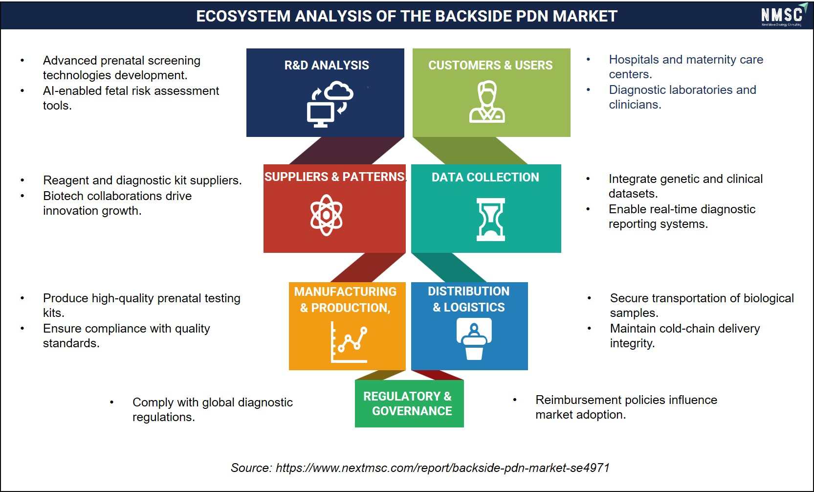
The ecosystem analysis highlights the interconnected value chain supporting advanced prenatal diagnostics and screening solutions. Innovation is driven by R&D activities focused on AI-enabled fetal risk assessment and enhanced screening technologies, while suppliers provide critical reagents and diagnostic components. Manufacturing ensures the production of high-quality, compliant testing kits, supported by efficient data collection systems that integrate genetic and clinical information. Distribution networks maintain sample integrity through secure logistics, while hospitals, maternity care centers, and diagnostic laboratories serve as key end users. Regulatory frameworks and reimbursement policies play a crucial role in ensuring compliance and driving market adoption.
Competitive Landscape
Competitive Dynamics and M&A Landscape
|
Key Takeaways |
Details |
|
Market Structure |
The Backside PDN Market is highly concentrated among a small number of globally leading semiconductor equipment OEMs, EDA platform vendors, and specialty materials suppliers. Applied Materials, Lam Research, and Tokyo Electron command the largest equipment revenue shares. Synopsys and Cadence dominate the EDA and Software and IP segment. |
|
Innovation Focus |
Innovation is concentrated in three parallel tracks: process equipment miniaturization for sub-2nm backside feature definition, EDA tool development for power integrity co-optimization with backside PDN architectures, and advanced materials development for ultra-low-resistance backside metallization and high-selectivity dielectrics. |
|
M&A Activity |
The competitive landscape has seen consolidation through strategic acquisitions targeting backside-relevant capabilities, including KLA's metrology portfolio expansion, Synopsys's acquisition of ANSYS to strengthen multiphysics simulation for thermal and power co-analysis, and ongoing equipment vendor investments in inspection and overlay capability for backside process control. |
How Do Companies Compete in the Backside PDN Market?
The market is characterized by intense competition on process performance specifications, tool integration capability, and application engineering depth. NMSC's analysis indicates that leading equipment suppliers including Applied Materials and Lam Research compete on the ability to deliver certified process modules for specific foundry backside PDN integration schemes rather than standalone tool metrics. EDA vendors Synopsys and Cadence compete on the comprehensiveness of their power integrity signoff platforms, with the ability to support design-technology co-optimization flows that incorporate foundry-specific backside PDN design rules becoming a critical competitive differentiator. Geographic expansion is focused on co-locating application engineering teams with advanced node fab customers in Taiwan, South Korea, and the United States to support qualification programs at TSMC, Samsung, and Intel.
Which Kind of Companies Dominate the Backside PDN Market?
Our findings suggest that the Backside PDN Market is dominated by large, diversified semiconductor equipment and EDA platform companies with the technical breadth and financial resources to develop and qualify multiple interconnected process steps within an integrated backside PDN process flow. Applied Materials, Lam Research, KLA Corporation, and Tokyo Electron hold dominant positions in equipment due to their ability to supply comprehensive wafer preparation, deposition, etch, and metrology solutions that foundries can qualify as coordinated process modules. Synopsys and Cadence dominate the software and IP segment due to their comprehensive EDA platform coverage, existing foundry PDK partnerships, and the high switching costs associated with changing signoff tools mid-process development cycle.
AI-Native Differentiation and Open Standards Drive Market Success in the Backside PDN Market
Based on NMSC's research, we found that companies demonstrating differentiated capability in AI-assisted process control and automated defect classification are gaining competitive advantage in backside PDN equipment qualification programs. The complexity of backside process integration, with multiple interdependent steps that must be simultaneously optimized for yield, creates strong demand for AI-augmented process control systems that can detect subtle process drift before it generates yield loss. EDA vendors embedding AI-driven power integrity analysis and automated PDN optimization suggestions within their signoff platforms are capturing stronger adoption among design teams managing the increased complexity of co-optimizing frontside signal routing alongside backside power distribution networks.
Market Players to Opt for Merger and Acquisition Strategies to Expand Their Presence in the Backside PDN Market
Our assessment indicates that strategic M&A activity is accelerating as established semiconductor equipment and EDA companies seek to fill portfolio gaps in backside PDN-specific capabilities through targeted acquisitions. The Synopsys-ANSYS combination, which received regulatory clearance in 2024, directly strengthens Synopsys's multiphysics simulation capability for thermal and power co-analysis critical to backside PDN signoff. Equipment vendors are acquiring specialized process chemistry and materials companies to gain control of the full consumables supply chain for backside metallization and CMP process steps. EV Group's continued investment in bonding and debonding equipment positions it as a consolidation candidate or potential acquiree for larger equipment groups seeking to complete their backside handling process portfolios.
Who Are the Key Market Players in the Backside PDN Market?
-
Applied Materials, Inc.
-
Tokyo Electron Limited
-
Lam Research Corporation
-
KLA Corporation
-
Synopsys, Inc.
-
Cadence Design Systems, Inc.
-
Siemens AG
-
ASM International N.V.
-
DISCO Corporation
-
EV Group GmbH
-
EBARA Corporation
-
Onto Innovation Inc.
-
SCREEN Holdings Co., Ltd.
-
SUSS MicroTec SE
-
Advantest Corporation
-
Veeco Instruments Inc.
-
MKS Instruments, Inc.
-
Entegris, Inc.
-
Shin-Etsu Chemical Co., Ltd.
-
Brewer Science, Inc.
What Are the Latest Developments in the Backside PDN Industry?
|
Date |
Event |
|
May 2026 |
EV Group and IMEC demonstrated wafer-to-wafer hybrid bonding with 200nm interconnect pitch and record overlay accuracy. Hybrid bonding is a critical enabling technology for future backside-interconnect and BSPDN-enabled 3D integration schemes. |
|
Apr 2025 |
Cadence expanded its collaboration with Intel Foundry and certified its digital and analog design solutions for Intel 18A. The company explicitly stated that its solutions are optimized for Intel 18A/18A-P technologies, including RibbonFET and PowerVia backside power delivery network architectures. |
|
Apr 2025 |
Synopsys and Intel Foundry expanded collaboration for Intel 18A and 18A-P, providing certified EDA flows optimized for Intel’s PowerVia backside power delivery technology. |
|
Mar 2025 |
EV Group launched the next-generation GEMINI automated wafer bonding platform. Wafer bonding is a key enabling process for advanced wafer thinning, backside processing, and future BSPDN integration flows used in advanced logic manufacturing. |
Expert Insights
 “We believe that combining backside power delivery with buried power rails – a structural scaling booster in the form of a local power rail that is buried deep in the chip’s front-end-of-line – is the most promising implementation scheme of a backside power delivery network in terms of scalability and performance.”
— Naoto Horiguchi, Director CMOS Device Technology at imec
The statement was made while discussing imec's demonstration of a backside power delivery architecture that combines buried power rails (BPRs), nano-through-silicon vias (nTSVs), and backside metallization to improve power distribution and enable continued logic scaling for future semiconductor nodes.
Market Interpretation
This insight highlights the semiconductor industry's increasing focus on Backside Power Delivery Networks (BSPDNs) as a critical enabler for sub-2nm and Angstrom-era process technologies. By integrating buried power rails with backside routing, manufacturers can separate power and signal interconnects, thereby reducing routing congestion, lowering IR drop, and improving overall chip performance and power efficiency. The statement underscores the growing industry belief that BSPDN architectures will play a foundational role in sustaining transistor scaling, supporting advanced AI processors, high-performance computing (HPC) devices, and next-generation logic technologies.
What Are the Investment Opportunities in the Backside PDN Market?
Capital Inflows and Advanced Packaging Investments
The Backside PDN Market is attracting significant investment as semiconductor manufacturers transition toward advanced node technologies and high-performance computing architectures. Major foundries and integrated device manufacturers are allocating substantial capital toward next-generation process technologies that incorporate backside power delivery networks. We observed that growing demand for AI accelerators, data center processors, high-performance GPUs, and advanced mobile chipsets is accelerating investments in process innovations designed to improve power efficiency, transistor density, and chip performance. Increasing funding across advanced packaging, chiplet architectures, and sub-2nm process technologies further supports long-term growth opportunities within the market.
Semiconductor Manufacturing Infrastructure Investment
Semiconductor fabrication facility expansion remains a foundational growth driver for the Backside PDN Market. Leading manufacturers are investing hundreds of billions of dollars in advanced fabrication plants, EUV lithography infrastructure, and next-generation process development. We found that investments in 2nm and below process nodes are increasingly incorporating backside power delivery architectures to address power integrity challenges and improve transistor scaling efficiency. These capital-intensive programs directly expand manufacturing capacity for advanced logic devices while creating substantial opportunities for equipment suppliers, materials providers, and semiconductor technology developers participating in the Backside PDN ecosystem.
Sustainable Semiconductor Manufacturing Initiatives
Environmental, Social, and Governance (ESG) considerations are increasingly influencing semiconductor manufacturing investments. Backside PDN architectures contribute to improved energy efficiency by reducing power loss, lowering voltage drop, and enhancing overall chip performance per watt. Semiconductor manufacturers are investing in process technologies that support sustainability objectives through reduced energy consumption and improved resource utilization. As governments and investors place greater emphasis on sustainable technology development, advanced semiconductor solutions incorporating backside power delivery technologies are expected to benefit from long-term investment prioritization.
AI, High-Performance Computing, and Digital Infrastructure Enablement
Backside PDN technology serves as a critical enabler for next-generation AI computing, cloud infrastructure, edge computing, and high-performance data processing applications. Organizations investing in artificial intelligence, hyperscale data centers, autonomous systems, and advanced networking infrastructure increasingly require processors capable of delivering higher performance with improved power efficiency. We further analyzed that the growing deployment of generative AI workloads, large language models, and advanced computing platforms is creating durable, multi-year demand for semiconductor technologies incorporating backside power delivery architectures.
Strategic Partnerships and M&A Activity
Strategic partnerships, technology licensing agreements, and targeted acquisitions are becoming increasingly important within the Backside PDN Market. Semiconductor manufacturers, equipment vendors, EDA software providers, and advanced materials companies are collaborating to accelerate commercialization of backside power delivery technologies. We assessed that investors should closely monitor developments involving advanced process integration, wafer fabrication technologies, semiconductor materials innovation, and packaging ecosystem consolidation. Companies possessing proprietary expertise in power delivery optimization, advanced lithography, process integration, and semiconductor design enablement are expected to remain attractive strategic investment and acquisition targets throughout the forecast period.
Key Benefits for Stakeholders
For Enterprise Buyers
Enterprise buyers gain comprehensive and vendor-neutral insights into the Backside PDN Market, including technology adoption trends, semiconductor process evolution, manufacturing roadmaps, and application-level demand forecasts. This intelligence supports strategic sourcing decisions, semiconductor procurement planning, and long-term technology investment strategies. Competitive analysis enables buyers to assess supplier capabilities, technology readiness, and ecosystem maturity across the advanced semiconductor value chain.
For Investors and Financial Analysts
Investors and financial analysts gain access to a structured assessment of the Backside PDN Market's growth outlook, technology adoption trajectory, competitive landscape, and investment opportunities through the forecast period. Segment-level analysis across applications, end-use industries, and geographic markets supports valuation modeling and portfolio construction. Detailed company assessments and technology tracking provide an early-indicator framework for identifying emerging leaders, strategic acquisition targets, and long-term growth opportunities within the advanced semiconductor industry.
For Semiconductor Manufacturers and Technology Providers
Semiconductor manufacturers, foundries, equipment suppliers, EDA vendors, and materials providers gain actionable intelligence regarding high-growth opportunities, technology commercialization pathways, and competitive positioning within the Backside PDN Market. Process technology analysis highlights emerging opportunities across AI processors, HPC chips, mobile SoCs, and advanced computing platforms. Regional and ecosystem analysis enables companies to prioritize investment decisions, strengthen technology partnerships, and optimize go-to-market strategies across the semiconductor value chain.
For Government and Regulatory Bodies
Government agencies, industry development organizations, and semiconductor policy stakeholders gain structured insights into how semiconductor investment programs, advanced manufacturing initiatives, supply chain resilience strategies, and technology sovereignty objectives are influencing the Backside PDN Market. Country-level perspectives support evidence-based policymaking related to semiconductor competitiveness, research and development funding, domestic manufacturing capacity expansion, and advanced technology ecosystem development. The analysis provides direct relevance to national semiconductor strategies and long-term digital infrastructure planning.
Supply Chain Structure of the Backside PDN Market
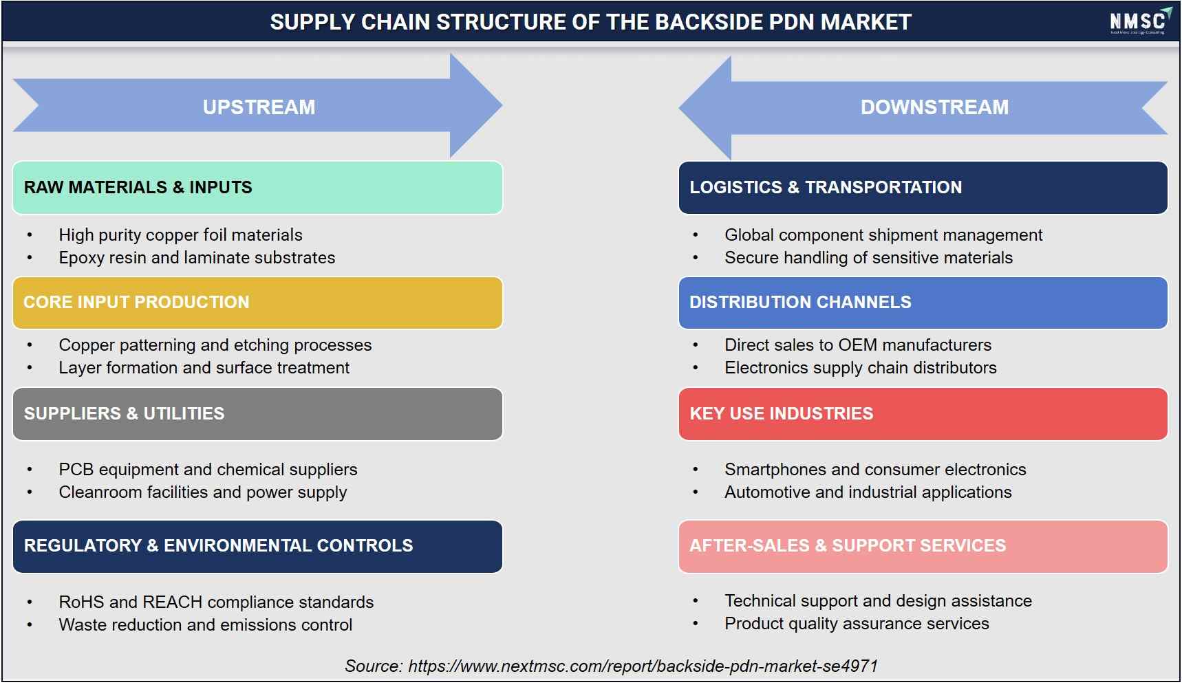
The supply chain structure of the Backside PDN market encompasses a well-integrated network of raw material providers, manufacturers, distributors, and end-use industries. Upstream activities focus on sourcing high-purity copper foils, laminates, and specialized chemicals, supported by equipment suppliers and regulatory compliance frameworks. Manufacturing processes involve precision copper patterning, etching, and surface treatment to produce advanced semiconductor substrates. Downstream operations include secure logistics, distribution to OEMs and electronics manufacturers, and application across smartphones, consumer electronics, automotive, and industrial sectors. After-sales services, including technical support and quality assurance, further strengthen market efficiency and customer satisfaction.
Key Market Segments
By Component
-
Equipment
-
Wafer Preparation Equipment
-
Grinding and Thinning
-
Polishing and Planarization
-
-
Backside Patterning Equipment
-
Lithography
-
Etch
-
Coat and Develop
-
Other Patterning
-
-
Backside Metallization Equipment
-
Barrier and Seed Deposition
-
Electroplating
-
Annealing
-
-
Bonding and Handling Equipment
-
Temporary Bonding
-
Debonding
-
Carrier Handling
-
-
Metrology and Inspection Equipment
-
Overlay and Alignment
-
Defect Inspection
-
Thickness Metrology
-
-
Test Equipment
-
Electrical Test
-
Failure Analysis
-
Characterization
-
-
Other Equipment
-
-
Materials and Consumables
-
Wafers and Substrates
-
Silicon Wafers
-
Silicon-on-Insulator Wafers
-
Engineered Substrates
-
Handle Wafers and Carriers
-
-
Bonding Materials
-
Temporary Bond Materials
-
Release Layers
-
Debond Chemicals
-
-
Dielectric Materials
-
Low-K Dielectrics
-
Passivation Dielectrics
-
Isolation Layers
-
-
Patterning Materials
-
Photoresists
-
Underlayers
-
Anti-Reflective Coatings
-
-
Metallization Materials
-
Barrier Materials
-
Seed Materials
-
Plating Chemistries
-
Solder Materials
-
-
CMP and Cleaning Consumables
-
Slurries
-
Pads
-
Clean Chemistries
-
-
Process Gases
-
Other Materials
-
-
Software and IP
-
EDA and Signoff
-
Power Integrity
-
Thermal Analysis
-
Physical Verification
-
Parasitic Extraction
-
-
IP and PDKs
-
Standard Cells
-
Interface IP
-
Memory IP
-
-
DTCO and Modeling
-
Other Software and IP
-
-
Services
-
Design Services
-
Process Development
-
Qualification and Characterization
-
Research and Development Consortia
-
Other Services
-
By Architecture
-
Buried Power Rail
-
Backside Via
-
Direct Backside Contact
-
Full Backside PDN
-
Other Architecture
By Technology Node
-
3 Nanometers and Below
-
4 Nanometers to 5 Nanometers
-
Above 5 Nanometers
-
Research and Pilot
By End Use
-
HPC and AI
-
Mobile
-
Client Computing
-
Automotive
-
Industrial and IoT
-
Other End Use
By Customer Type
-
Foundry
-
IDM
-
Fabless
-
OSAT
-
Research Institute
-
Other Customer
By Sales Channel
-
Direct
-
Distributor
-
Partner
-
OEM
-
Other Channel
By Region
-
North America: U.S., Canada, and Mexico.
-
Europe: UK, Germany, France, Italy, Spain, Sweden, Denmark, Finland, the Netherlands, and the rest of Europe.
-
Asia Pacific: China, India, Japan, South Korea, Taiwan, Indonesia, Vietnam, Australia, Philippines, Malaysia and the rest of APAC.
-
Middle East & Africa (MEA): Saudi Arabia, UAE, Egypt, Israel, Turkey, Nigeria, South Africa, and the rest of MEA.
-
Latin America: Brazil, Argentina, Chile, Colombia, and the rest of LATAM.
Conclusion and Recommendations
Long-Term Outlook
The Backside PDN Market is at the beginning of a decade-long structural growth cycle driven by the fundamental necessity of backside power delivery for competitive semiconductor performance at 3nm and below. The market is forecast to grow from USD 1.5 billion in 2026 to USD 8.6 billion by 2035 at a CAGR of 21.8%, reflecting both the scaling of volume production at leading-edge nodes and the progressive broadening of the customer base from a handful of advanced foundries to a wider ecosystem of IDMs, OSATs, and research institutions. Our analysis shows that this growth is durable rather than cyclical, as no alternative to backside power delivery has been identified that resolves the IR drop and routing congestion challenges at sub-3nm logic nodes.
Strategic Positioning Recommendations
Equipment vendors should invest in modular backside PDN process toolsets that can be qualified as integrated sequences rather than individual tools, as foundry customers are increasingly procuring coordinated backside process solutions rather than point tools. EDA vendors should prioritize power-signal co-optimization platform capabilities and foundry PDK partnerships for backside process design rules, as design teams will require tightly integrated frontside-backside analysis to achieve competitive results at advanced nodes. Materials suppliers should build deep application engineering relationships with leading foundries early in process qualification cycles, as first-mover qualification positions create durable revenue streams that are difficult for competitors to displace once a backside process flow is in production.
Investment Attractiveness
The Backside PDN Market represents a compelling investment environment characterized by high barriers to entry, long customer qualification cycles that create recurring revenue visibility, and strong secular demand growth linked to the most important megatrend in the global economy: AI compute expansion. Our assessment indicates that the highest-conviction investment themes within the market include Software and IP tools (25.1% CAGR), Research Institute customers (28.5% CAGR), Direct Backside Contact architecture (24.3% CAGR), and OSAT customer development (31.2% CAGR). Investors should monitor consolidation activity among specialty equipment and materials vendors as larger strategic buyers seek to complete their backside PDN portfolio coverage ahead of the volume production ramp at leading foundries.
Market Shifts and Key Risks
The most significant market shift underway is the transition from research-phase equipment procurement by a small number of advanced foundries to commercial-scale process qualification and volume production across a broader set of leading-edge logic manufacturers. This shift accelerates the Backside PDN Market revenue ramp but also increases competitive intensity among equipment and materials suppliers competing for qualification slots. Key risks include potential delays in advanced node ramp schedules at TSMC, Samsung, and Intel due to yield challenges, escalating export control restrictions that constrain equipment supplier market access, and the theoretical risk of an alternative power delivery innovation that reduces the perceived necessity of full backside PDN implementation.
Growth Pathways
Organizations seeking to maximize value from the Backside PDN Market should pursue a phased engagement strategy aligned with technology readiness milestones. In the near term through 2027, prioritize engagement with research consortia including IMEC programs to establish technology familiarity and early customer relationships ahead of production qualification. In the mid-term from 2027 to 2031, focus resources on production qualification at leading foundry customers in Taiwan and South Korea where volume ramp will generate the largest near-term revenue opportunities. In the long term from 2031 to 2035, position for expanded customer base coverage as the technology propagates from leading-edge foundries to IDMs, advanced OSATs, and second-tier fabs adopting backside PDN for their node transition programs.
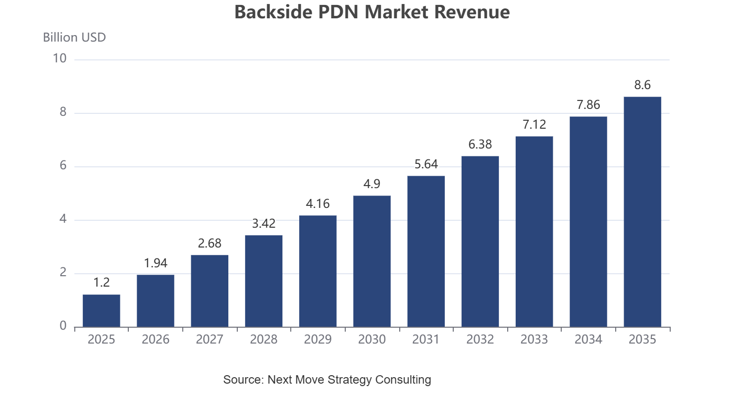
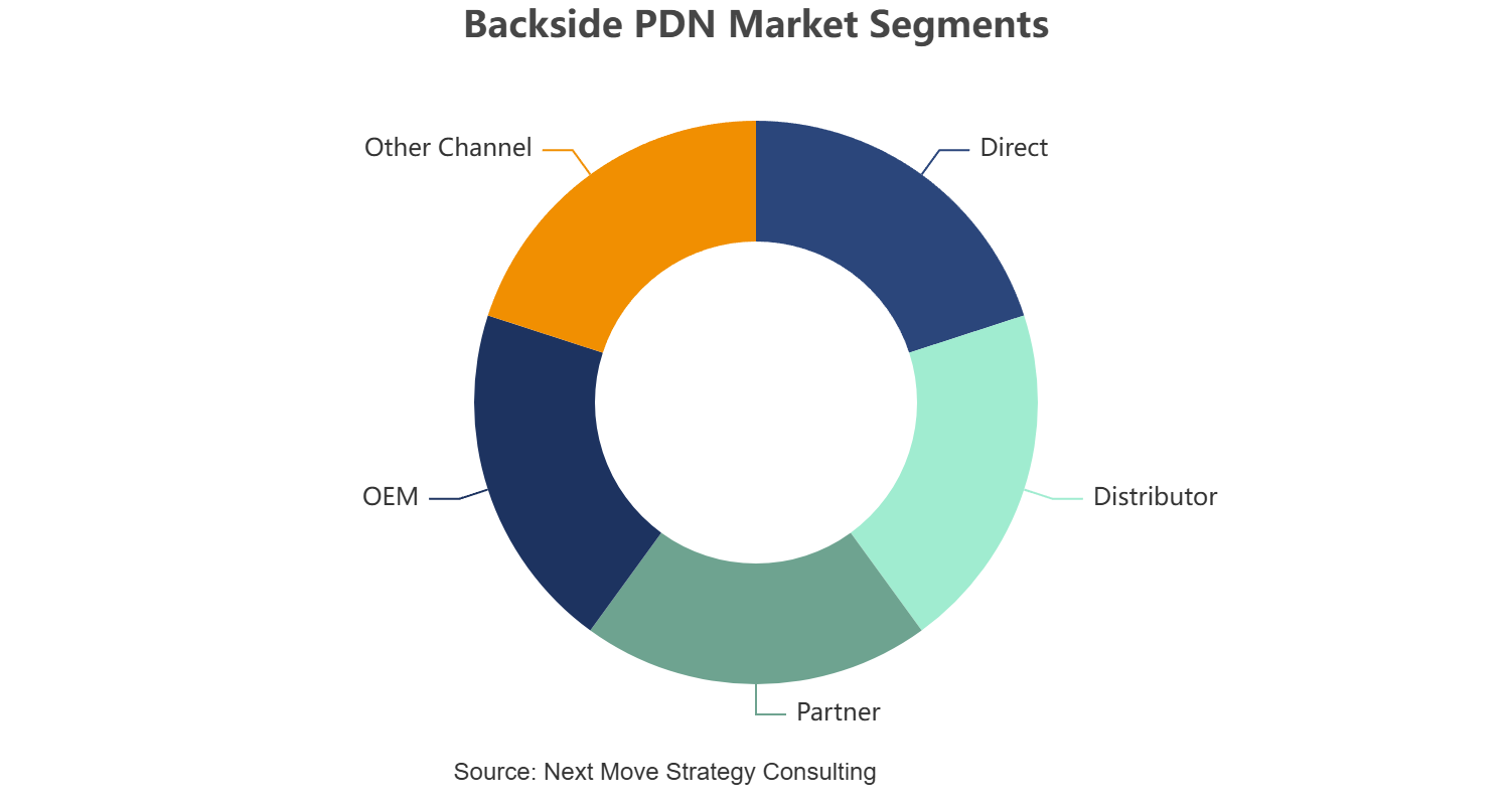
About the Author
 Mihul Sharma
— Mihul Sharma is Research Associate at Next Move Strategy Consulting, where he has covered technology, industrial, and healthcare markets for 3 years. His work applies structured business research, market analysis, and secondary-source review to assess market trends, competitive developments, and growth opportunities. He supports report development by fully synthesizing industry data, company information, and market signals into concise findings for strategy and investment-focused research teams.
Mihul Sharma
— Mihul Sharma is Research Associate at Next Move Strategy Consulting, where he has covered technology, industrial, and healthcare markets for 3 years. His work applies structured business research, market analysis, and secondary-source review to assess market trends, competitive developments, and growth opportunities. He supports report development by fully synthesizing industry data, company information, and market signals into concise findings for strategy and investment-focused research teams.
About the Reviewer
 Supradip Baul
— Supradip Baul is an accomplished business consultant and strategist with over a decade of rich experience in market intelligence, strategy, technology, and business transformation. His work has included rigorous qualitative and quantitative analysis across multiple industries, helping clients shape investment decisions and long-term roadmaps. Earlier in his career, he was associated with Gartner, where he contributed to industry-leading reports and market share analyses. He has worked with leading global companies and holds an MBA with a dual specialization in Marketing and Finance.
Supradip Baul
— Supradip Baul is an accomplished business consultant and strategist with over a decade of rich experience in market intelligence, strategy, technology, and business transformation. His work has included rigorous qualitative and quantitative analysis across multiple industries, helping clients shape investment decisions and long-term roadmaps. Earlier in his career, he was associated with Gartner, where he contributed to industry-leading reports and market share analyses. He has worked with leading global companies and holds an MBA with a dual specialization in Marketing and Finance.
At Next Move Strategy Consulting, we understand that insightful market research is the cornerstone of successful business decisions. That's why we employ a robust and multifaceted approach, combining various methodologies to deliver the most accurate and actionable data for our clients.

Research Landscape
We navigate the world of research with two primary approaches:
Qualitative Approach
Our qualitative research methodologies involve immersive techniques such as in-depth interviews, focus groups, and observational studies. By engaging directly with individuals and stakeholders, we uncover valuable insights that quantitative data alone may overlook.

Quantitative Research
In tandem with qualitative methodologies, NMSC leverages the power of Quantitative Research to provide a robust foundation of numerical insights. Through systematic data collection and analysis, we quantify patterns, preferences, and market trends, offering a comprehensive view of the business landscape.
Our quantitative research approach employs diverse tools, including surveys, experiments, and statistical modelling. These methodologies enable us to gather data from a large and representative sample, ensuring the statistical significance of our findings. By employing structured questionnaires and standardized data collection methods, we guarantee the reliability and validity of the information we present to our clients.
Quantitative research is particularly effective in measuring the prevalence of trends, assessing market size, and gauging the impact of various factors on consumer behavior. The numerical precision attained through this approach equips our clients with actionable insights, facilitating data-driven decision-making and strategy formulation.


Our Specialized Toolbox for Industry-Specific Market Research
We deploy a specialized arsenal of techniques tailored to meet your unique requirements. Here's a glimpse into our comprehensive toolbox:

Information Procurement
The stage entails acquiring market data or relevant information through various sources and methodologies.


Market Research Approach
We utilize both top-down and bottom-up approaches in market research analysis to achieve a comprehensive understanding of the market dynamics, leveraging the broad perspective of industry trends and macroeconomic factors alongside detailed insights from specific segments and individual companies.

Porters Five Forces Analysis
We conduct Porter's Five Forces analysis to evaluate the competitive landscape of an industry, providing us with insights into factors that affect profitability and strategic positioning.
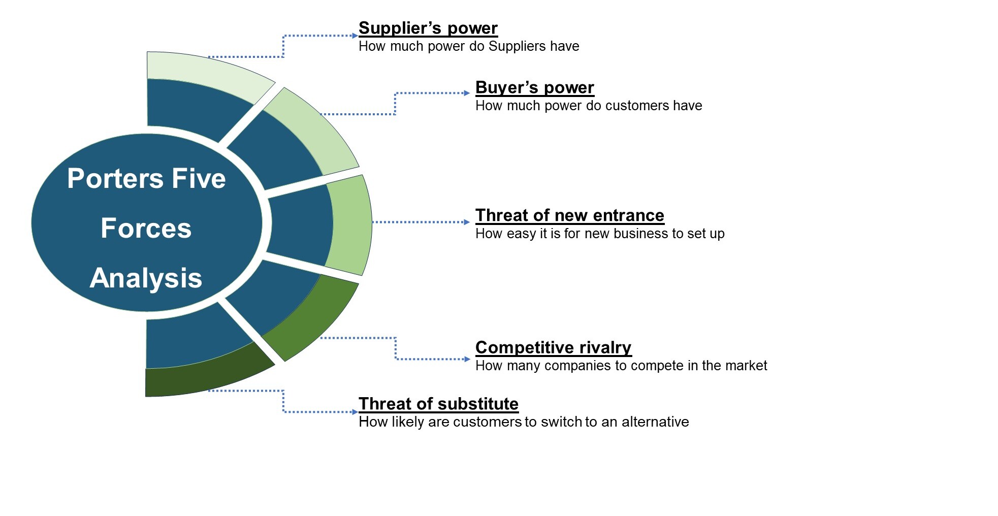
SWOT Analysis

Forecasting
We utilize a forecasting model to predict future consumption by considering parameters like population, economics, regulations, market competition, drivers, constraints, technology, and pricing. We also employ statistical techniques such as multilinear regression, exponential smoothing, moving average, ARIMA, and Monte Carlo simulations for accurate predictions. In econometric forecasting, we analyzed short-term and long-term event impacts, attributing values based on regulatory frameworks, economic factors, and market events.





 Speak to Our Analyst